 | –≠–ª–µ–∫—Ç—Ä–æ–Ω–Ω—ã–π –∫–æ–º–ø–æ–Ω–µ–Ω—Ç: STA310 | –°–∫–∞—á–∞—Ç—å:  PDF PDF  ZIP ZIP |
1/90
STA310
June 2003
This is preliminary information on a new product now in development. Details are subject to change without notice.
1
FEATURES
s
DVD Audio
decoder:
Meridian Lossless Packing
(
MLP
), with
up to 6 channels,
Uncompressed LPCM with 1-8 channels,
Precision of up to 24 bits and sample rates
of between 44.1 kHz and 192 kHz.
s
Dolby Digital
(*)
decoder:
Decodes 5.1
Dolby Digital Surround.
Output up to 6 channels. downmix modes:
1, 2, 3 or 4 channels.
s
MPEG -1 2- channel audio decoder, layers I and
II.
s
MPEG-2 6-channel audio decoder, layer II.
24 bits decoding precision.
s
MP3 (MPEG layer III) decoder.
s
Accepts MPEG-2 PES stream format for:
MPEG-2, MPEG-1, Dolby Digital and linear
PCM.
s
Karaoke System.
s
Prologic decoder.
s
Downmix for Dolby Prologic compatible.
A separate (2-ch) PCM output available for
simultaneous playing and recording.
s
Bitstream input interface: serial, parallel or
SPDIF.
s
SPDIF and IEC-61937 input interface.
s
SPDIF and IEC-61937 output interface.
s
PLL for internal PCM clock generation.
frequencies supported: 44.1KHz family (22.05,
88.2, 176.4) and 48KHz family (24, 48, 96, 192).
s
PCM: transparent, downsampling 192 to 96 Khz
and 96 to 48kHz.
s
PTS handling control on-chip.
s
No external DRAM required
s
I
2
C or parallel control bus
s
Embedded
Development RAM
for
customizable software capability.
s
Configurable internal PLLs for system and
audio clocks, from an externally provided clock.
s
80-PIN TQFP package
s
2.5V (for core) and 3V (for I/O) power supply.
3V Capable I/O Pads .
s
True-SPDIF input receiver supporting AES/
EBU, IEC958, S/PDIF.
No external chip required.
Differential or single ended inputs can be
decoded.
APPLICATIONS
s
High-end audio equipment.
s
DVD consumer players.
s
Set top box.
s
HDTV .
s
Multimedia PC.
(*) "Dolby ", "AC-3" and "ProLogic" are
trademarks of Dolby Laboratories.
DESCRIPTION
The STA310 is a fully integrated Audio Decoder ca-
pable of decoding all the above listed formats.
Encoded input data can be entered either by a serial
(I2S or SPDIF) or a parallel interface. A second input
data stream (I2S) is available for micro input.
The control interface can be either I
2
C or a parallel 8-
bit interface. No external DRAM is necessary for a to-
tal of 35ms surround delays.
TQFP80
ORDERING NUMBER: STA310
PRELYMINARY DATA
6+2-CH. MULTISTANDARD AUDIO DECODER
STA310
2/90
2
STA310 AUDIO DECODER PIN DESCRIPTION
Pin Number
Name
Type
Function
CONTROL INTERFACES
48
IRQB
O
(1)
Interrupt Signal (level), active low
47
SELI2C
I
(2)
Selects the Control Interface (when high: serial interface; when
low: parallel interface)
I
2
C Control Interface
43
SDAI2C
I/O
(1)
I
2
C Serial Data
46
SCLKI2C
I
I
2
C Clock
53
MAINI2CADR
I
(2)
Determines the slave address
Parallel Control Interface
78 - 79 - 80 - 1
2 - 3 - 6 - 7
D0 - D1 - D2 - D3
D4 - D5 - D6 - D7
I/O
Host Data
12 - 13 - 14 - 15
16 - 18 - 19 - 20
A0 - A1 - A2 - A3
A4 - A5 - A6 - A7
I
Host Address
21
DCSB
I
Chip Select, active low
22
R/W
I
Read/Write Selection: read access when high, write access
when low
35
WAITB
O
(3)
Data Acknowledge, active low
DATA INPUT INTERFACE
First Serial Data Interface (I
2
S)
37
DSTRB
I
Clock Input Data, active low
41
SIN
I
Serial Input Data
40
LRCLKIN
I
Word Clock for the Input
42
REQ
O
Handshake for the Data Transfer, aconfigurable by the
SIN_SETUP register
Second Serial Data Interface (I
2
S)
62
DSTRB2
I
Clock Input Data, active low
60
SIN2
I
Serial Input Data
61
LRCLKIN2
I
Word Clock for the Input
63
REQ2
O
Handshake for the Data Transfer, active low
DATA OUTPUT INTERFACES
69
PCMCLK
I/O
Oversampling Clock input for STA310 when generated externally
DAC Interface
67
SCLK
O
Bit Clock for the DAC
3/90
STA310
68
LRCLK
O
Word Clock for the DAC
72
PCM_OUT0
O
Data from a Prologic downmix (VCR_L/VCR_R)
73
PCM_OUT1
O
Data for the first DAC (Left/Right)
76
PCM_OUT2
O
Data for the second DAC (Centre/Sub)
77
PCM_OUT3
O
Data for the third DAC (LeftSur/RightSur)
IEC958 Interface (S/PDIF) - One Output Port., One Input Ports.
58
I958OUT
O
S/PDIF Signal
25
SPDP
I
First differential input of S/P DIF port
24
SPDN
I
Second differential input of S/P DIF port
26
SPDF
I
External Filter
28
VDDA
I
Analog VDD for S/P DIF Input port
29
GNDA
I
Analog GND for S/P DIF Input port
STATUS INFORMATION
PCM Related Information
54
SFREQ
O
Then high, indicates that the sampling freq. is either 44.1Khz or
22.05Khz.
When low, indicates that the sampling frequency is either 32 Khz,
48 Khz, 24 Khz or 16Khz.
57
DEEMPH
O
Indicates if de-emphasis is performed.
Audio Video Synchronization
59
PTSB
O
Indicates that a PTS has been detected, active low.
Other Signals
31
CLK
I
Master Clock Input Signal.
36
RESET
I
(2)
Reset signal input, active low.
52
TESTB
I
(2)
Reserved pin: to be connected to VDD
49
SMODE
I
Reserved pin : to be connected to GND
RS232 Interface
8
RS232RX
I
9
RS232TX
O
PLLs INTERFACES
64
CLKOUT
O
System clock output with programmable division ratio
27
PLLAF
I
External Filter For Audio PLL.
2
STA310 AUDIO DECODER PIN DESCRIPTION (continued)
Pin Number
Name
Type
Function
STA310
4/90
Notes
(1) Open Drain
(2) Internal Pull-up
(3) Tri-State
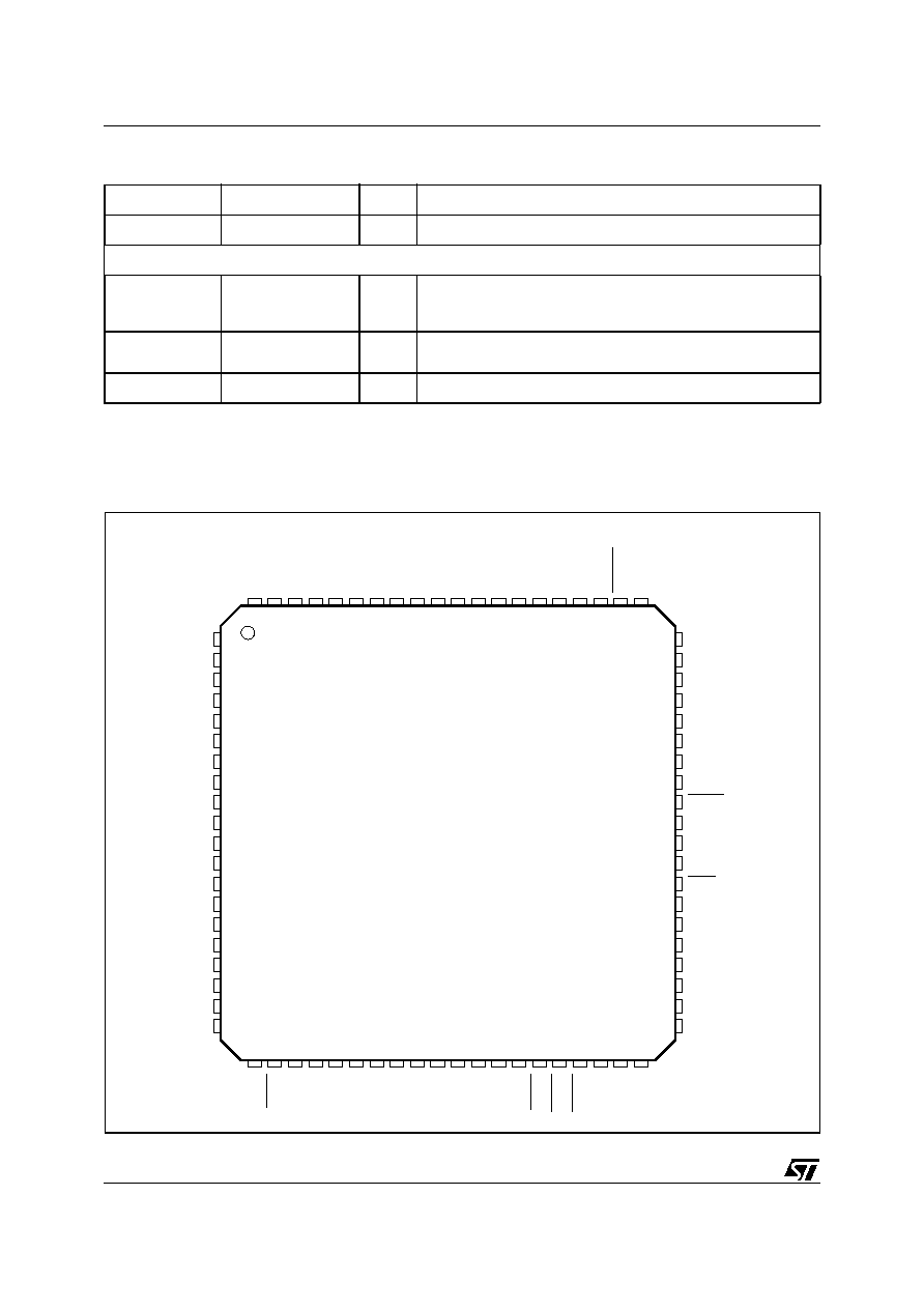
PIN CONNECTION (Top view)
30
PLLSF
I
External Filter For System PLL.
Power and Ground
5 - 11 - 23 - 33 -
39 - 45 - 50 - 56
- 66 - 71 - 75
GND
GND
Ground
4 - 17 - 34 - 38
44 - 55 - 65 - 74
VDD
VDD
2.5V Power Supply
10 - 32 - 51 - 70
VDD3
VDD3
3.3V Power Supply
2
STA310 AUDIO DECODER PIN DESCRIPTION (continued)
Pin Number
Name
Type
Function
1
2
3
5
6
4
7
8
9
10
31
11
32 33 34 35 36
75 74 73 72
70
71
69 68 67 66 65
55
54
53
51
50
52
60
59
58
56
57
D6
GND
VDD
D4
D3
D5
GND
VDD3
RS232TX
D7
RS232RX
SPDF
PLLAF
VDDA
GNDA
CLK
PLLSF
VDD3
GND
VDD
WAITB
HRSTB
GND
VDD
PCM_OUT1
PCM_OUT0
VDD3
GND
PCMCLK
LRCLK
SCLK
GND
VDD
VDD
SFREQ
MAINI2CADD
VDD3
GND
TESTB
SIN2
PTSB
I958OUT
GND
DEEMPH
D00AU1225
26 27 28 29 30
76
PCM_OUT2
77
PCM_OUT3
78
D0
79
D1
80
D2
DCSB
HRWB
GND
SPDN
SPDP
21 22 23 24 25
49
48
46
45
47
SMODE
IRQB
SCLKI2C
GND
SELI2C
12
13
14
15
16
A4
A3
A2
A0
A1
64 63 62 61
CLKOUT
REQ2
DSTRB2
LRCLKIN2
37 38 39 40
DSTRB
VDD
GND
LRCKLIN
44
42
41
43
VDD
REQ
SIN
SDAI2C
17
18
19
20
A7
A6
A5
VDD
5/90
STA310
ABSOLUTE MAXIMUM RATINGS
ELECTRICAL CHARACTERISTICS (V
DD
= 3.3V +/-0.3V; T
amb
= 0 to 70∞C; Rg = 50
unless otherwise spec-
ified
GENERAL INTERFACE
Note: 1. The leakage currents are generally very small, <1nA. The value given here, 1
µ
A, is a maximum that can occur after an Electrostatic
Stress on the pin.
2. V> Vdd3 for 3.3V buffers.
3. Human Body Model
LVTTL & LVCMOS DC Input Specification 2.7V <Vdd3 <3.6V
Note: 1. Takes into account 200mV voltage drop in both supply lines.
2. X in the source/sink current under worst case conditions and is reflected in the name of the I/O cell according to the drive capability
Symbol
Parameters
Value
Unit
Vdd
2.5V Power Supply Voltage
-0.5 to 3.3
V
2.5V Input or Output Voltage
-0.5 to (Vdd+0.5)
V
Vdd3
3.3V Power Supply Voltage
-0.5 to 4
V
3.3V Input or Output Voltage
-0.5 to (Vdd+0.5)
V
DC OPERATING CONDITIONS
Symbol
Parameters
Value
Unit
Vcc
Power Supply Voltage
2.5
V
Tj
Operating Junction Temperature
-20 to 125
∞C
Symbol
Parameters
Conditions
Min
Typ
Max
Unit
Note
I
il
Low level input current without
pull-up device
Vi = 0V
1
µ
A
1
I
ih
High level input current without
pull-down device
Vi = Vdd
1
µ
A
1
I
oz
Tri-state output leakage without
pull-up/down device
Vi = 0V or Vdd
1
µ
A
1
I
latchup
I/O Latch-up current
V<0V, V>Vdd
200
mA
2
Vesd
Electrostatic protection
Leakage <1
µ
A
2000
V
3
Symbol
Parameters
Conditions
Min
Typ
Max
Unit
Note
V
il
Low level input voltage
0.8
V
1
V
ih
High level input voltage
2.0
V
1
V
ilhyst
Low level threshold input falling
0.8
1.35
V
1
V
ihhyst
High level threshold input rising
1.3
2.0
V
1
V
hyst
Schmitt trigger hysteresis
0.3
0.8
V
1