 | –≠–ª–µ–∫—Ç—Ä–æ–Ω–Ω—ã–π –∫–æ–º–ø–æ–Ω–µ–Ω—Ç: STA450A | –°–∫–∞—á–∞—Ç—å:  PDF PDF  ZIP ZIP |
1/66
STA450A
September 2003
FUNCTIONS
s
XMRADIO SERVICE LAYER
DEMULTIPLEXING
s
CHANNEL AUXILIARY DATA MANAGEMENT
s
CONDITIONAL ACCESS CONTROL
s
SERVICE COMPONENTS EXTRACTION
s
SERVICE COMPONENTS DECRYPTION
s
HIGH QUALITY AUDIO DECODING WITH
DATA RATE FROM 24kbps TO 96kbps
s
HIGH QUALITY SPEECH DECODING WITH
DATA RATE FROM 4kbps TO 16kbps
s
44.1 AND 32KHz SAMPLING FREQUENCIES
SUPPORTED
s
SYNCHRONIZATION ERROR DETECTION
WITH SW INDICATORS
PERIPHERALS
s
HIGH SPEED SERIAL INPUT INTERFACE
(PCBITSTREAM INTERFACE)
s
FULLY PROGRAMMABLE SERIAL PCM
OUTPUT INTERFACE
s
IEC958 OUTPUT (S/PDIF)
s
DATA OUTPUT PORT INTERFACE
s
CONDITIONAL ACCESS PROCESSOR
INTERFACE (I2C MASTER)
s
RS232 RX & TX INTERFACES
s
EMBEDDED SYSTEM PLL
s
EMBEDDED AUDIO PLL
LOW POWER TECHNOLOGY
s
1.8V 0.18
µ
m TECHNOLOGY
s
3.3V CAPABLE I/Os
CONTROL
s
I2C SLAVE CONTROL
s
DEVICE ADDRESS: 1011100
DESCRIPTION
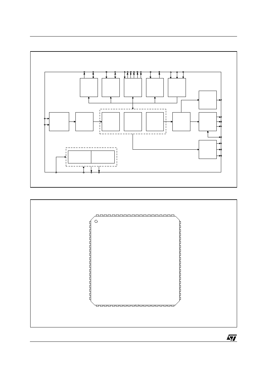
The STA450A is designed for digital radio receivers
compatible with the XMRadio SDARS System and in-
tegrates all the functions needed to perform the Ser-
vice Layer and Source Decoding:
≠ Bitstream Synchronization
≠ Service Layer (SL) Demultiplexing
≠ Auxiliary Data Management
≠ Conditional Access (CA) Control
≠ Service Components Extraction
≠ Service Components Decryption
≠ Audio and Voice Decoding
The extracted Audio and Data are made available
through different interfaces:
≠ I2S Audio Output
≠ S/PDIF Output
≠ Data Output Port
TQFP80
ORDERING NUMBER: STA450A
T H I S D E V I C E C A N B E S O L D O N LY TO
CUSTOMERS THAT HAVE SIGNED A LICENSE
AGREEMENT WITH XM SATELLITE RADIO.
XMRADIO
Æ
SDARS SERVICE LAYER & SOURCE DECODER
STA450A
2/66
Figure 1. Service Layer and Source Decoder Block Diagram
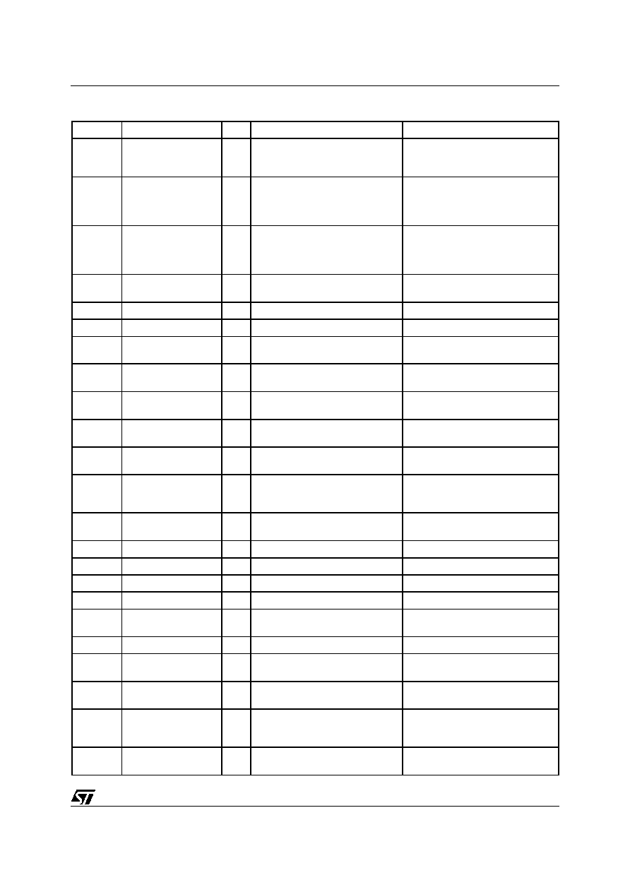
Figure 2. Pin Connection
INPUT
BUFFER
OUTPUT
BUFFER
AUDIO PORT
OUTPUT
INTERFACE
(PCM I/F)
SPDIFF
OUTPUT
SERVICE
LAYER DEMUX
DECRYPTION
AUDIO
DECODER
DSP BASED
RS232
I2C MASTER
(CAP I/F)
I2C SLAVE
(SYSCON I/F)
GPIO
INTERFACE
EXTERNAL
INTERRUPT
LRCKT
OCLK
SCKT
SDO
I958_OUT
R
S
232_TX
R
S
232_R
X
S
C
L_M
SDA_
M
SCL
SDA
PC BITSTREAM
INPUT
INTERFACE
(USSIO 0)
PCDC
PCSD
DATA PORT
OUTPUT
INTERFACE
(USSIO 3)
DP_EN
DP_CLK
DP_DATA
1 LI
N
E
N
U
EVENT_
I
R
Q
CAP_
RST
SYS PLL
AUDIO PLL
SYSTEM & AUDIO CLOCKS
RESET_
N
CL
K_
I
N
CL
K_
O
U
T
FI
LT_0
PCFS
7 LI
N
E
S
N
U
PL
L
_
SYNC
IN
T
1
IN
T
2
TEST
1
2
3
5
6
4
7
8
9
10
31
11
32 33 34 35 36
75 74 73 72
70
71
69 68 67 66 65
55
54
53
51
50
52
60
59
58
56
57
CAP_RST (GPIO_4)
NU (GPIO_5)
SD
O
L
R
CKT
TQFP80
26 27 28 29 30
76
77
78
79
80
P
LL_
S
Y
N
C
(
F
I
T
_5)
CL
K_
M
1
SCK
T
21 22 23 24 25
49
48
46
45
47
12
13
14
15
16
SCL_M
64 63 62 61
V
DD1
0
37 38 39 40
N
U
(U
SSIO
0
_
L
R
C
L
K
)
44
42
41
43
17
18
19
20
VDD1
GND1
DP
_
E
N
R
S
232
_TX
VDD1
2
GND
1
0
APLL_GND
FI
LT_
0
CLK_OUT
TEST1
CLK_IN
TEST0
VDD2
GND2
VDD_IO1
SDA_M
VDD3
GND3
SCL
SDA
APLL_VDD
NU
VD
D4
GND
4
CL
K
_
M
0
NU (
R
EQ)
VDD5
GND
5
VDD_
I
O
2
P
C
FS
(
F
I
T
_2)
VDD6
GN
D
6
NU (
F
I
T
_
1
)
GND7
VDD7
GND8
VDD8
VDD_IO3
RESET_N
GND9
VDD9
NU (IT_0)
G
ND1
2
OCL
K
DP
_
D
A
T
A
D
P
_C
LK
IN
T
1
(
G
PI
O
_
1
)
VDD1
1
GND1
1
VD
D_
I
O
4
NU (USSIO1_LRCLK)
EVENT_IRQ (GPIO_0)
R
S
23
2_R
X
I
9
58_
O
U
T
NU (IT_1)
SCAN_MODE
N
U
(
F
IT
_
3
)
NU (IT_2)
TESTB
NU (FIT_0)
NU (
F
I
T
_
4
)
PC
DC
PCS
D
NU (USSIO1_DATA)
NU (USSIO1_SCLK)
NU (USSIO2_LRCLK)
NU (USSIO2_DATA)
NU (USSIO2_SCLK)
IN
T2
(
G
PIO
_
2
)
TE
S
T
(
G
P
I
O
_
3
)
3/66
STA450A
PIN FUNCTION
N∞
Pin
Type
Function
Pad Description
1,6,53
NU(IT_1),
NU(IT_2),
NU(IT_0)
I
Not Used (must be connected to
ground in functional mode)
Schmitt Trigger Buffer
2,9,15,23,
30,37,44,5
0,57,62,69
,76
GND1...,GND12
Ground
3,10,16,
24,31,38,4
5,51,58,63
,70,77
VDD1...,VDD12
1.8V Core Supply Voltage
4
TEST0
I
Test Pin (must be connected to
ground in functional mode)
Analog Pad
5
CLK_IN
I
Clock Input
Schmitt Trigger Buffer
7
TESTB
I
Test Pin
Input Pad Buffer with Active Pull-Up
8
CAP_RST (GPIO_4)
I/O
CAP Reset
Bi Dir Pad, 4mA Output Buffer with
Slew Rate Control
11,32,52,7
1
VDD_IO1,...
VDD_IO4
3.3V I/O Supply Voltage
12
CLK_OUT
O
Clock Out
4mA Output Buffer with Slew Rate
Control
13
SCL_M
O
I2C Master Serial Clock
4mA Output Buffer with Slew Rate
Control
14
SDA_M
I/O
I2C Master Serial Data
Bi Dir Pad, 4mA Output Buffer with
Slew Rate Control
17,27,28,4
0
NU(FIT_0),
NU(FIT_3),
NU(FIT_4), NU(FIT_1)
I
Not Used (must be connected to
ground in functional mode)
Schmitt Trigger Buffer
18
SCAN_MODE
I
Scan Mode (must be connected to
ground in functional mode)
Input Pad Buffer
19
APLL_GND
Analog Ground for Audio PLL
20
APLL_VDD
1.8V Analog Supply for Audio PLL
21
FILT_0
PLL Filter
Analog Pad
22
NU
Not Used
25,26
CLK_M1, CLK_M0
I
Selection of Input Clock for the DSP
core and peripherals
Input Pad Buffer
29
PLL_SYNC (FIT_5)
I
Fractional Audio PLL Sync.
Schmitt Trigger Buffer
33
PCDC
I/O
PC Bitstream Data Clock
Schmitt Trigger Bi Dir Pad, 4mA
Output Buffer with Slew Rate Control
34
PCSD
I/O
PC Bitstream Serial Data
Schmitt Trigger Bi Dir Pad, 4mA
Output Buffer with Slew Rate Control
35,41,46
NU(USSIO0_LRCLK)
NU(USSIO1_LRCLK)
NU(USSIO2_LRCLK)
I/O
Not Used (must be connected to
ground in functional mode)
Schmitt Trigger Bi Dir Pad, 4mA
Output Buffer with Slew Rate Control
36
NU(REQ)
O
Not used
4mA Output Buffer with Slew Rate
Control
STA450A
4/66
A more detailed description of each pad type can be found in section 4.
Note: After an Hardware reset or power on all Bi Dir pins are configured as inputs.
39
PCFS(FIT_2)
I
PC Bitstream PRC Frame Sync.
Schmitt Trigger Buffer
42,47
NU(USSIO1_DATA)
NU(USSIO2_DATA)
I/O
Not Used (must be connected to
ground in functional mode)
Schmitt Trigger Bi Dir Pad, 4mA
Output Buffer with Slew Rate Control
43,48
NU(USSIO1_SCLK)
NU(USSIO2_SCLK)
I/O
Not Used (must be connected to
ground in functional mode)
Schmitt Trigger Bi Dir Pad, 4mA
Output Buffer with Slew Rate Control
49
NU(GPIO_5)
I/O
Not Used (must be connected to
ground in functional mode)
Bi Dir Pad, 4mA Output Buffer with
Slew Rate Control
54
TEST1
I
Test Pin
Input Pad Buffer with Active Pull-Up
55
RESET_N
I
HW Reset (active low)
Schmitt Trigger Buffer
56
EVENT_IRQ
(GPIO_0)
I/O
General Interrupt (Events, Errors,
Data ready)
Bi Dir Pad, 4mA Output Buffer with
Slew Rate Control
59
SCL
I
I2C Slave Serial Clock
Schmitt Trigger Buffer
60
SDA
I/O
I2C Slave Serial Data
BiDir Pad, 4mA Output Buffer with
Slew Rate Control
61
INT1 (GPIO_1)
I/O
Dedicated Errors Interrupt
Bi Dir Pad, 4mA Output Buffer with
Slew Rate Control
64
INT2 (GPIO_2)
I/O
Dedicates Events Interrupt
Bi Dir Pad, 4mA Output Buffer with
Slew Rate Control
65
TEST (GPIO_3)
I/O
Test Pin
Bi Dir Pad, 4mA Output Buffer with
Slew Rate Control
66
DP_EN
I/O
Data Port Enable
Schmitt Trigger Bi Dir Pad, 4mA
Output Buffer with Slew Rate Control
67
DP_DATA
I/O
Data Port Data
Schmitt Trigger Bi Dir Pad, 4mA
Output Buffer with Slew Rate Control
68
DP_CLK
I/O
Data Port Clock
Schmitt Trigger Bi Dir Pad, 4mA
Output Buffer with Slew Rate Control
72
LRCKT
O
I2S Left&Right Clock
4mA Output Buffer with Slew Rate
Control
73
SDO
O
I2S Output Data (PCM Data)
4mA Output Buffer with Slew Rate
Control
74
SCKT
O
I2S Serial Clock
4mA Output Buffer with Slew Rate
Control
75
OCLK
I/O
Oversampling Clock
Schmitt Trigger BiDir Pad, 4mA
Output Buffer with Slew Rate Control
78
I958_OUT
O
S/PDIF Output
4mA Output Buffer with Slew Rate
Control
79
RS232_TX
O
RS232 Transmitter
4mA Output Buffer with Slew Rate
Control
80
RS232_RX
I
RS232 Receiver (must be
connected to ground in functional
mode)
Schmitt Trigger Buffer
PIN FUNCTION (continued)
N∞
Pin
Type
Function
Pad Description
5/66
STA450A
ABSOLUTE MAXIMUM RATINGS
THERMAL DATA
DC ELECTRICAL CHARACTERISTCS (T
amb
= -40 to 85∞C, V
DD
= APLL_V
DD
= 1.65 to 1.95V, V
DD_IO
= 3.0
to 3.6V unless otherwise specified).
Symbol
Parameter
Value
Unit
V
DD
1.8V Power supply Voltage
-0.5 to 2.5
V
V
DD_IO
3.3V Power Supply Voltage
-0.5 to 4
V
APLL_V
DD
1.8V Analog Supply Voltage
-0.5 to 2.5
V
V
i
Voltage on input pin
-0.5 to (V
DD_IO
+ 0.5)
V
V
o
Voltage on output pin
-0.5 to (V
DD_IO
+ 0.5)
V
T
stg
Storage temperature
-55 to +150
∫C
T
oper
Operative Ambient Temperature
-40 to +85
∫C
T
j
Operative Junction Temperature
-40 to +125
∫C
Symbol
Parameter
Value
Unit
R
j-amb
Thermal Resistance Junction to Ambient
(1)
(1)
According to JEDEC specification on a 4 layers board
40
∞C/W
Symbol
Parameter
Conditions
Min
Typ
Max
Unit
V
DD
1.8V Supply Voltage
1.65
1.8
1.95
V
V
DD_IO
3.3V Supply Voltage
3.0
3.3
3.6
V
APLL_V
DD
1.8V Analog Supply Voltage
1.65
1.8
1.95
V
I
DD
V
DD
Power Supply Current
f
CLK
= 23.92MHz; 56kbps
audio stream; V
DD
=1.95V
110
140
mA
I
DD_IO
V
DD_IO
Power Supply Current
f
CLK
= 23.92MHz; 56kbps
audio stream; V
DD_IO
=3.6V;
V
DD
=1.95V
24
40
mA
I
DD_APLL
APLL_V
DD
Power Supply Current
f
CLK
= 23.92MHz;
APLL_V
DD
=1.95V
0.5
1.2
mA
P
D
Power Dissipation
V
DD
= 1.8V; V
DD_IO
= 3.3V
220
mW
I
il
Low level input leakage current
4)
Vi = 0V
1
µ
A
I
ih
High level input leakage current
4)
Vi = V
DD3
1
µ
A
I
OZ
Tristare output leakage current
5)
Vo = 0V or V
DD3
1
µ
A
I
pu
Pull-up current
Vi = 0V
40
120
µ
A
R
pu
Equivalent pull-up resistance
3)
Vi = 0V
50
k
V
il
Low level input voltage
0.8
V
V
ih
High level input voltage
2
V
V
ilhyst
Low level threshold input falling
0.8
1.35
V
V
ihhyst
High level threshold input rising
1.3
2
V
V
hyst
Schmitt trigger hysteresy
1)
0.3
0.8
V