1/8
STA502
September 2003
s
MINIMUM INPUT OUTPUT PULSE WIDTH
DISTORTION
s
200m
R
dsON
COMPLEMENTARY DMOS
OUTPUT STAGE
s
CMOS COMPATIBLE LOGIC INPUTS
s
THERMAL PROTECTION
s
THERMAL WARNING OUTPUT
s
UNDER VOLTAGE PROTECTION
DESCRIPTION
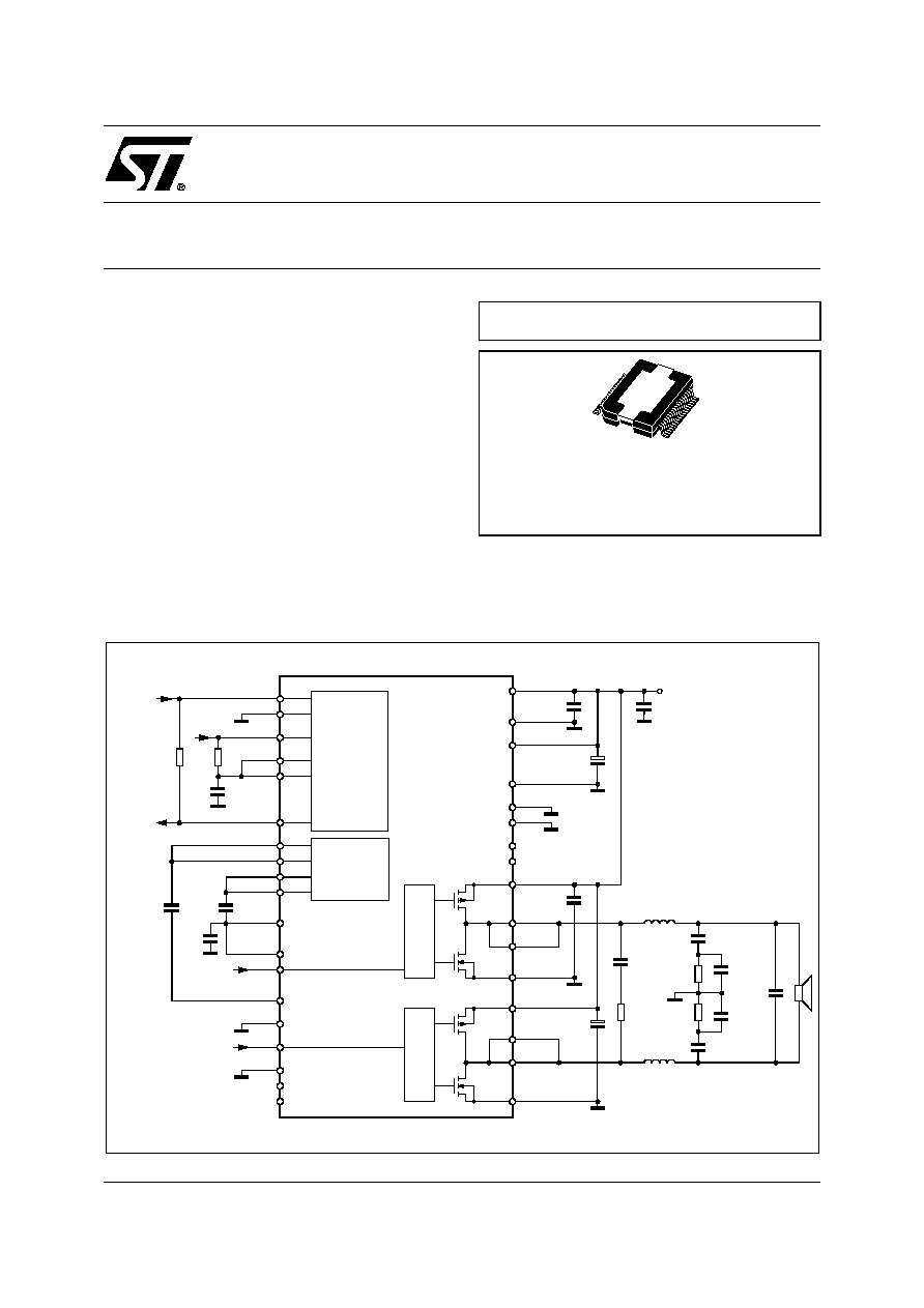
STA502 is a monolithic dual half bridge stage in Mul-
tipower BCD Technology.
The device is particularly designed to make the out-
put stage of a mono All-Digital High Efficiency
(DDXTM) amplifier capable to deliver 60W @ THD =
10% at V
cc
32V output power on 8
load. The input
pins have threshold proportional to Ibias pin voltage.
PowerSO36
ORDERING NUMBER: STA502
40V 4A DOUBLE POWER HALF BRIDGE
AUDIO APPLICATION CIRCUIT
C30
1
�
F
C107
100nF
C106
100nF
C55
1000
�
F
C58
100nF
C58
100nF
R57
10K
R59
10K
C53
100nF
C60
100nF
C31
1
�
F
R104
20
C109
330pF
15
GND
IBIAS
CONFIG
PWRDN
PWRDN
FAULT
TRI-STATE
TH_WAR
TH_WAR
+3.3V
GND
V
DD
V
DD
V
SS
V
SS
V
CC
SIGN
V
CC
SIGN
GND-Reg
GND-Clean
INA
INA
INB
PROTECTIONS
&
LOGIC
REGULATORS
29
23
24
25
27
26
28
30
21
22
33
34
35
36
GND
V
CC
14
12
GND
V
CC
B
13
L113 22
�
H
L112 22
�
H
C32
1
�
F
+V
CC
C108
470nF
C33
1
�
F
7
M17
M15
M16
M14
8
9
OUTA
GNDA
OUTA
V
CC
A
6
4
2
3
OUTB
GNDB
D02AU1447
OUTB
V
CC
B
5
N.C.
N.C.
16
17
19
31
20
GNDSUB
1
N.C.
10
N.C.
11
INB
32
C110
100nF
C111
100nF
R103
6
R102
6
MULTIPOWER BCD TECHNOLOGY
STA502
2/8
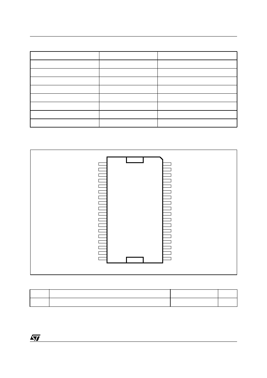
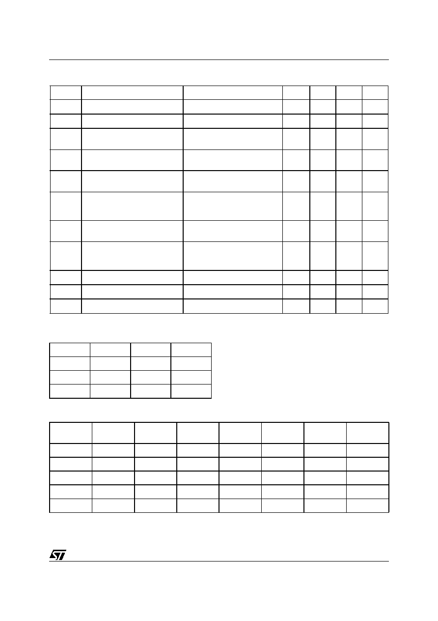
PIN FUNCTION
N�
Pin
Description
1
GND-SUB
Substrate ground
35 ; 36
Vcc Sign
Signal Positive supply
15
V
CC
Positive Supply
12
V
CC
Positive Supply
7
V
CC
Positive Supply
4
V
CC
Positive Supply
14
GND
Negative Supply
13
GND
Negative Supply
6
GND
Negative Supply
5
GND
Negative Supply
16 ; 17
N.C.
10 ; 11
N.C.
8 ; 9
OUTA
Output half bridge
2 ; 3
OUTB
Output half bridge
29
GND
30
GND
31
INA
Input of half bridge
32
INB
Input of half bridge
21 ; 22
Vdd
5V Regulator referred to ground
33 ; 34
V
SS
5V Regulator referred to + V
CC
25
PWRDN
Stand-by pin
26
TRI-STATE
Hi-Z pin
27
FAULT
Fault pin advisor
24
GND
28
TH-WAR
Thermal warning advisor
19
GND-Clean
Logical ground
23
IBIAS
High logical state setting voltage
18
NC
Not connected
20
GND-Reg
Ground for regulator Vdd
3/8
STA502
FUNCTIONAL PIN STATUS
* : The pin is open collector. To have the high logic value, it needs to be pulled up by a resistor.
PIN CONNECTION
THERMAL DATA
PIN NAME
Logical value
IC -STATUS
FAULT
0
Fault detected (Short circuit, or Thermal ..)
FAULT *
1
Normal Operation
TRI-STATE
0
All powers in Hi-Z state
TRI-STATE
1
Normal operation
PWRDN
0
Low absorpion
PWRDN
1
Normal operation
THWAR
0
Temperature of the IC =130�C
THWAR*
1
Normal operation
Symbol
Description
Value
Unit
R
th j-case
Thermal Resistance Junction-case
max 1.5
�C/W
GND-SUB
OUTB
OUTB
V
CC
GND
V
CC
GND
N.C.
N.C.
GND-Reg
VDD
VDD
GND
IBIAS
V
SS
V
SS
V
CC
Sign
V
CC
Sign
18
16
17
15
6
5
4
3
2
21
22
31
32
33
35
34
36
20
1
19
N.C.
GND-Clean
D02AU1449
N.C
V
CC
N.C.
PWRDN
FAULT
TRI-STATE
9
8
7
28
29
30
OUTA
TH_WAR
10
27
GND
OUTA
V
CC
GND
INB
GND
14
12
11
23
25
26
GND
INA
13
24
STA502
4/8
ABSOLUTE MAXIMUM RATINGS
THERMAL DATA
ELECTRICAL CHARACTERISTCS (I
bias
= 3.3V; V
CC
= 30V; T
amb
= 25�C unless otherwise specified)
Symbol
Parameter
Value
Unit
V
CE
DC Supply Voltage (Pin 4,7,12,15)
40
V
V
max
Maximum Voltage on pins 23 to 32
5.5
V
P
tot
Power Dissipation (T
case
= 70�C)
50
W
T
op
Operating Temperature Range
0 to 70
�C
T
stg
, T
j
Storage and Junction Temperature
-40 to 150
�C
Symbol
Parameter
Min.
Typ.
Max.
Unit
T
j-case
Thermal Resistance Junction to Case (thermal pad)
2.5
�C/W
T
jSD
Thermal shut-down junction temperature
150
�C
T
warn
Thermal warning temperature
130
�C
t
hSD
Thermal shut-down hysteresis
25
�C
Symbol
Parameter
Test conditions
Min.
Typ.
Max.
Unit
R
dsON
Power Pchannel/Nchannel
MOSFET RdsON
Id=1A;
200
270
m
I
dss
Power Pchannel/Nchannel
leakage Idss
V
CC
=35V;
50
�
A
g
N
Power Pchannel RdsON
Matching
Id=1A;
95
%
g
P
Power Nchannel RdsON
Matching
Id=1A;
95
%
Dt_s
Low current Dead Time (static)
see test circuit no.1; see fig. 1
10
20
ns
Dt_d
High current Dead Time (dinamic) L=22
�
H; C = 470nF; Rl = 8
Id=3.5A; see fig. 3
50
ns
t
d ON
Turn-on delay time
Resistive load
100
ns
t
d OFF
Turn-off delay time
Resistive load
100
ns
t
r
Rise time
Resistive load; as fig.1
25
ns
t
f
Fall time
Resistive load; as fig. 1
25
ns
V
CC
Supply voltage operating voltage
10
36
V
V
IN-H
High level input voltage
Ibias/2
+300mV
V
V
IN-L
Low level input voltage
Ibias/2
-300mV
V
I
IN-H
Hi level Input current
Pin voltage = Ibias
1
�
A
5/8
STA502
Notes: 1. The following table explains the VL, VH variation with Ibias
LOGIC TRUTH TABLE (see fig. 2)
I
IN-L
Low level input current
Pin voltage = 0.3V
1
�
A
I
PWRDN-H
Hi level PWRDN pin input current
Ibias = 3.3V
35
�
A
V
L
Low logical state voltage VL (pin
PWRDN, TRISTATE) (note 1)
Ibias = 3.3V
0.8
V
V
H
High logical state voltage VH (pin
PWRDN, TRISTATE) (note 1)
Ibias = 3.3V
1.7
V
I
VCC-
PWRDN
Supply current from Vcc in Power
Down
PWRDN = 0
3
mA
I
FAULT
Output Current pins
FAULT -TH-WARN when
FAULT CONDITIONS
Vpin = 3.3V
1
mA
I
VCC-hiz
Supply current from Vcc in Tri-
state
Tri-state=0;
22
mA
I
VCC
Supply current from Vcc in
operation
(both channel switching)
Input pulse width = 50% Duty;
Switching Frequency = 384KHz;
No LC filters;
80
mA
I
VCC-q
Isc (short circuit current limit)
4
6
8
A
V
OUT-SH
Undervoltage protection threshold
7
V
V
OV
Output minimum pulse width
No Load
70
150
ns
Ibias
VLmin
VHmax
Unit
2.7
0.7
1.5
V
3.3
0.8
1.7
V
5
0.85
1.85
V
TRI-STATE
INA
INB
Q1
Q2
Q3
Q4
OUTPUT
MODE
0
x
x
OFF
OFF
OFF
OFF
Hi-Z
1
0
0
OFF
OFF
ON
ON
DUMP
1
0
1
OFF
ON
ON
OFF
NEGATIVE
1
1
0
ON
OFF
OFF
ON
POSITIVE
1
1
1
ON
ON
OFF
OFF
Not used
Symbol
Parameter
Test conditions
Min.
Typ.
Max.
Unit
ELECTRICAL CHARACTERISTCS (continued)