1/10
STA508
June 2004
1
FEATURES
MULTIPOWER BCD TECHNOLOGY
MINIMUM INPUT OUTPUT PULSE WIDTH
DISTORTION
200m
R
dsON
COMPLEMENTARY DMOS
OUTPUT STAGE
CMOS COMPATIBLE LOGIC INPUTS
THERMAL PROTECTION
THERMAL WARNING OUTPUT
UNDER VOLTAGE PROTECTION
2
DESCRIPTION
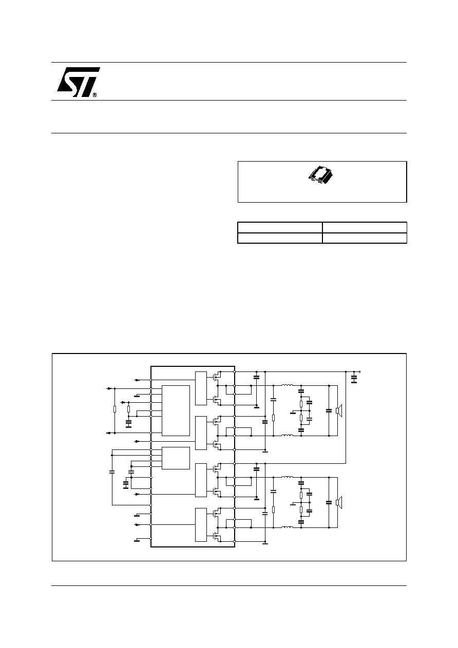
STA508 is a monolithic quad half bridge stage in Mul-
tipower BCD Technology. The device can be used as
dual bridge or reconfigured, by connecting CONFIG
pin to Vdd pin, as single bridge with double current
capability, and as half bridge (Binary mode) with half
current capability.
The device is particularly designed to make the out-
put stage of a stereo All-Digital High Efficiency
(DDXTM) amplifier capable to deliver 80 + 80W @
THD = 10% at V
cc
35V output power on 8
load.
In single BTL configuration is also capable to deliver
a peak of 160W @THD = 10% at V
CC
= 35V on 4
load (t
1sec). The input pins have threshold propor-
tional to Ibias pin voltage.
40V 4.5A QUAD POWER HALF BRIDGE
Figure 2. Block Diagram
L18 22
�
H
L19 22
�
H
C30
1
�
F
C20
100nF
C99
100nF
C101
100nF
C107
100nF
C106
100nF
C23
470nF
C55
1000
�
F
C21
100nF
C58
100nF
C58
100nF
R57
10K
R59
10K
R63
20
R98
6
R100
6
C53
100nF
C60
100nF
C31
1
�
F
C52
330pF
R104
20
C109
330pF
15
M3
IN1A
IN1A
V
L
CONFIG
PWRDN
PWRDN
FAULT
TRI-STATE
TH_WAR
TH_WAR
+3.3V
IN1B
V
DD
V
DD
V
SS
V
SS
V
CC
SIGN
V
CC
SIGN
GND-Reg
GND-Clean
IN2A
IN1B
IN2A
IN2B
PROTECTIONS
&
LOGIC
REGULATORS
29
23
24
25
27
26
28
30
21
22
33
34
35
36
M2
M5
M4
17
16
OUT1A
GND1A
OUT1A
V
CC
1A
14
12
10
11
OUT1B
GND1B
OUT1B
V
CC
1B
13
L113 22
�
H
L112 22
�
H
C32
1
�
F
+V
CC
C108
470nF
C33
1
�
F
7
M17
M15
M16
M14
8
9
OUT2A
GND2A
OUT2A
V
CC
2A
6
4
2
3
OUT2B
GND2B
D00AU1148B
OUT2B
V
CC
2B
5
19
31
20
GNDSUB
1
IN2B
32
C110
100nF
C111
100nF
R103
6
R102
6
8
8
REV. 2
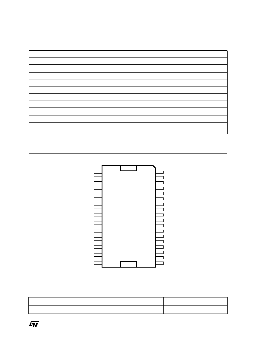
Figure 1. Package
Table 1. Order Codes
Part Number
Package
STA508
PowerSO36
PowerSO36
STA508
2/10
Table 2. Pin Description
N�
Pin
Description
1
GND-SUB
Substrate Ground
2 ; 3
OUT2B
Output Half Bridge 2B
4
V
CC
2B
Positive Supply
5
GND2B
Negative Supply
6
GND2A
Negative Supply
7
V
CC
2A
Positive Supply
8 ; 9
OUT2A
Output Half Bridge 2A
10 ; 11
OUT1B
Output Half Bridge 1B
12
V
CC
1B
Positive Supply
13
GND1B
Negative Supply
14
GND1A
Negative Supply
15
V
CC
1A
Positive Supply
16 ; 17
OUT1A
Output Half Bridge 1A
18
NC
Not Connected
19
GND-clean
Logical Ground
20
GND-Reg
Ground for Regulator V
dd
21 ; 22
V
dd
5V Regulator Referred to Ground
23
V
L
High Logical State Setting Voltage
24
CONFIG Configuration
pin
25
PWRDN
Stand-by pin
26
TRI-STATE
Hi-Z pin
27
FAULT
Fault pin Advisor
28
TH-WAR
Thermal Warning Advisor
29
IN1A
Input of Half Bridge 1A
30
IN1B
Input of Half Bridge 1B
31
IN2A
Input of Half Bridge 2A
32
IN2B
Input of Half Bridge 2B
33 ; 34
V
SS
5V Regulator Referred to +V
CC
35 ; 36
V
CC
Sign
Signal Positive Supply
3/10
STA508
Table 3. FUNCTIONAL PIN STATUS
(*) : The pin is open collector. To have the high logic value, it needs to be pulled up by a resistor.
(**): To put CONFIG = 1 means connect Pin 24 (CONFIG) to Pins 21, 22 (Vdd)
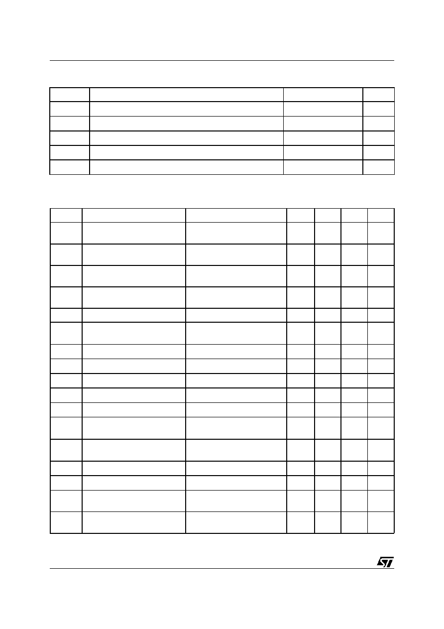
Figure 3. PIN CONNECTION
Table 4. THERMAL DATA
PIN NAME
Logical value
IC -STATUS
FAULT
0
Fault detected (Short circuit, or Thermal ..)
FAULT
(*)
1
Normal Operation
TRI-STATE
0
All powers in Hi-Z state
TRI-STATE
1
Normal operation
PWRDN
0
Low absorpion
PWRDN
1
Normal operation
THWAR
0
Temperature of the IC =130�C
THWAR
(*)
1
Normal operation
CONFIG
0
Normal Operation
CONFIG
(**)
1
OUT1A = OUT1B ; OUT2A=OUT2B
(IF IN1A = IN1B; IN2A = IN2B)
Symbol
Description
Value
Unit
R
th j-case
Thermal Resistance Junction-case
max 1.5
�C/W
GND-SUB
OUT2B
OUT2B
V
CC
2B
GND1B
V
CC
1A
GND1A
OUT1A
OUT1A
GND-Reg
VDD
VDD
CONFIG
V
SS
V
SS
V
CC
Sign
V
CC
Sign
18
16
17
15
6
5
4
3
2
21
22
31
32
33
35
34
36
20
1
19
N.C.
GND-Clean
D01AU1273
OUT1B
V
CC
1B
OUT1B
PWRDN
FAULT
TRI-STATE
9
8
7
28
29
30
OUT2A
TH_WAR
10
27
GND2B
OUT2A
V
CC
2A
IN1A
IN2B
IN1B
14
12
11
23
25
26
GND2A
IN2A
13
24
VL
STA508
4/10
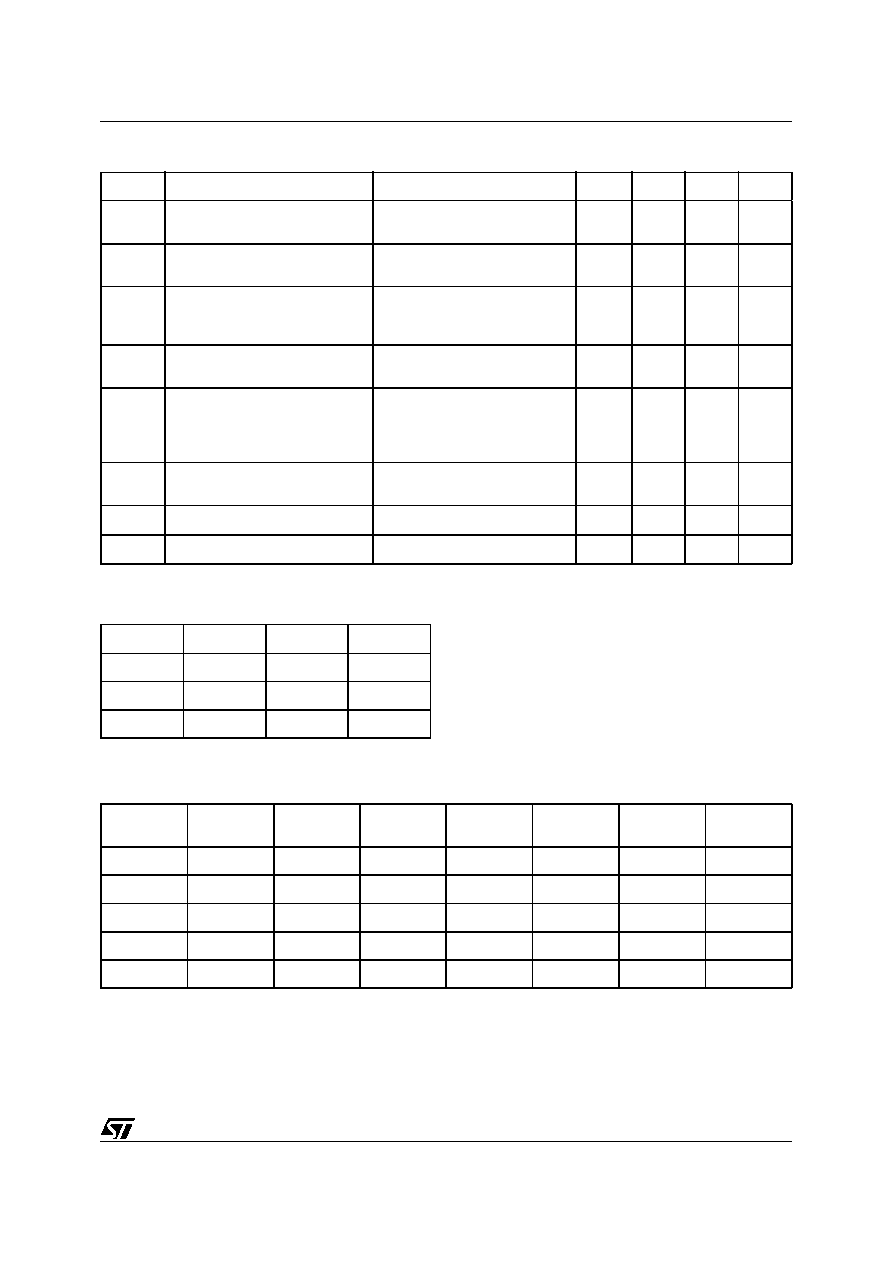
Table 5. ABSOLUTE MAXIMUM RATINGS
Table 6. ELECTRICAL CHARACTERISTCS (V
L
= 3.3V; V
CC
= 30V; T
amb
= 25�C ; f
sw
=384 unless
otherwise specified)
Symbol
Parameter
Value
Unit
V
CE
DC Supply Voltage (Pin 4,7,12,15)
40
V
V
max
Maximum Voltage on pins 23 to 32
5.5
V
P
tot
Power Dissipation (T
case
= 70�C)
50
W
T
op
Operating Temperature Range
0 to 70
�C
T
stg
, T
j
Storage and Junction Temperature
-40 to 150
�C
Symbol
Parameter
Test conditions
Min.
Typ.
Max.
Unit
R
dsON
Power Pchannel/Nchannel
MOSFET RdsON
Id=1A
200
270
m
I
dss
Power Pchannel/Nchannel
leakage Idss
V
CC
=35V
50
�
A
g
N
Power Pchannel RdsON
Matching
Id=1A
95
%
g
P
Power Nchannel RdsON
Matching
Id=1A
95
%
Dt_s
Low current Dead Time (static)
see test circuit no.1; see fig. 4
10
20
ns
Dt_d
High current Dead Time (dinamic) L=22
�
H; C = 470nF; R
L
= 8
Id=3.5A; see fig. 3
50
ns
t
d ON
Turn-on delay time
Resistive load
100
ns
t
d OFF
Turn-off delay time
Resistive load
100
ns
t
r
Rise time
Resistive load; as fig.4
25
ns
t
f
Fall time
Resistive load; as fig. 4
25
ns
V
CC
Supply voltage operating voltage
9
36
V
V
IN-High
High level input voltage
V
L
/2
+300mV
V
V
IN-Low
Low level input voltage
V
L
/2 -
300mV
V
I
IN-High
High level Input current
Pin Voltage = V
L
1
�
A
I
IN-Low
Low level input current
Pin Voltage = 0.3V
1
�
A
I
PWRDN-H
High level PWRDN pin input
current
V
L
= 3.3V
35
�
A
V
L
Low logical state voltage VL (pin
PWRDN, TRISTATE) (note 1)
V
L
= 3.3V
0.8
V
5/10
STA508
Table 7.
Notes: 1. The following table explains the VLow, VHigh variation with Ibias
Note 2: See relevant Application Note AN1994
Table 8. LOGIC TRUTH TABLE (see fig. 5)
V
H
High logical state voltage VH (pin
PWRDN, TRISTATE) (note 1)
V
L
= 3.3V
1.7
V
I
VCC-
PWRDN
Supply CURRENT from Vcc in
Power Down
PWRDN = 0
3
mA
I
FAULT
Output Current pins
FAULT -TH-WARN when
FAULT CONDITIONS
Vpin = 3.3V
1
mA
I
VCC-hiz
Supply Current from Vcc in Tri-
state
V
CC
= 30V; Tri-state = 0
22
mA
I
VCC
Supply Current from Vcc in
operation
both channel switching)
V
CC
=30V;
Input Pulse width = 50% Duty;
Switching Frequency = 384KHz;
No LC filters;
50
mA
I
VCC-q
Isc (short circuit current limit)
(note 2)
4.5
6
9
A
V
OUT-SH
Undervoltage protection threshold
7
V
V
OV
Output minimum pulse width
No Load
70
150
ns
V
L
VLow min
VHigh max
Unit
2.7
0.7
1.5
V
3.3
0.8
1.7
V
5
0.85
1.85
V
TRI-STATE
INxA
INxB
Q1
Q2
Q3
Q4
OUTPUT
MODE
0
x
x
OFF
OFF
OFF
OFF
Hi-Z
1
0
0
OFF
OFF
ON
ON
DUMP
1
0
1
OFF
ON
ON
OFF
NEGATIVE
1
1
0
ON
OFF
OFF
ON
POSITIVE
1
1
1
ON
ON
OFF
OFF
Not used
Symbol
Parameter
Test conditions
Min.
Typ.
Max.
Unit
Table 6. ELECTRICAL CHARACTERISTCS (continued)