 | –≠–ª–µ–∫—Ç—Ä–æ–Ω–Ω—ã–π –∫–æ–º–ø–æ–Ω–µ–Ω—Ç: STA510 | –°–∫–∞—á–∞—Ç—å:  PDF PDF  ZIP ZIP |

1/7
STA510
July 2003
This is preliminary information on a new product now in development. Details are subject to change without notice.
s
MINIMUM INPUT OUTPUT PULSE WIDTH
DISTORTION
s
150m
R
dsON
NDMOS OUTPUT STAGE
s
CMOS COMPATIBLE LOGIC INPUTS
s
THERMAL PROTECTION
s
WARNING OUTPUT: THERMAL, OVERLOAD
s
UNDER VOLTAGE PROTECTION ON V
REG
s
OVERVOLTAGE PROTECTION
s
TWO LEVELS CURRENT PROTECTION
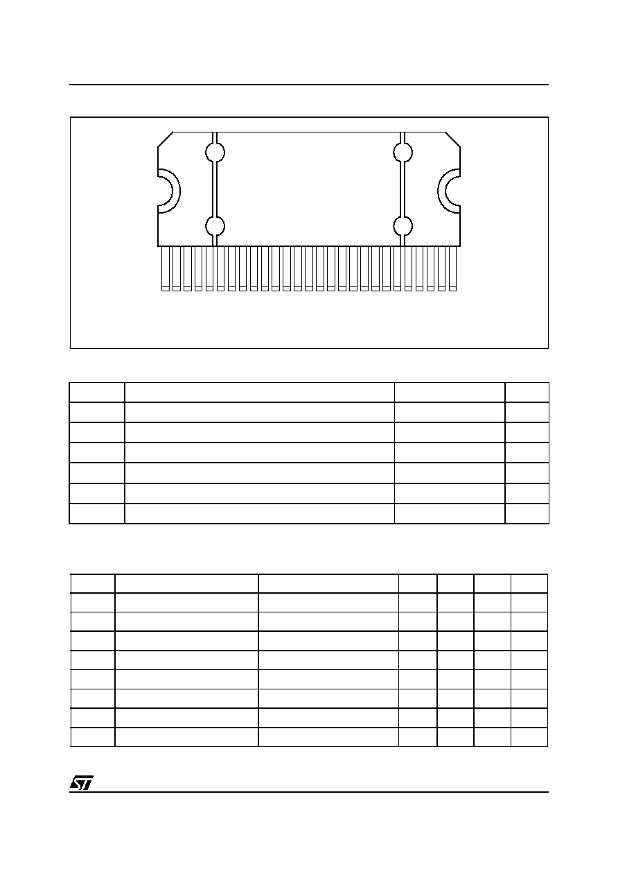
DESCRIPTION
STA510 is a monolithic full bridge stage in Multipow-
er BCD Technology. The device is particularly de-
signed to make the output stage of classD audio
amplifier capable to deliver 100W undistorted output
power on 8
load. The input pins have threshold pro-
portional to V
Ibias
pin voltage. The commutation
speed of the output stage is settable with an extenal
resistor (Curref pin) to choice for each application the
best compromise of THD versus EMI and current
spikes.
The overcurrent protection works in two steps, the
first one, at a lower value limits the current terminat-
ing the pulse (independently to the input) when the
current in the power output MOS reaches a first
threshold: it is aimed to act in case of overload and its
effect is to stabilize the mean current in the load to a
limit value. The second step shuts down completely
the device and restarts the power on sequence if the
current reaches a second (higher) threshold: it is
aimed to act in case of short circuit, when the first lim-
itation can fail.
Flexiwatt27
ORDERING NUMBER: STA510
PRODUCT PREVIEW
60V 5A POWER FULL BRIDGE
AUDIO APPLICATION CIRCUIT
R4
20
C11
1000
µ
F
VCCL
BOOTL
C5
330pF
C3 100nF
C4
100nF
C6
100nF
R5
6
OUTL
Q1
10
11
9
7
SUB
14
12
13
19
21
DRIVER
L
PROTECTIONS
&
LOGIC
REGULATOR
Q3
V
CC
D03AU1508
TRISTATE
+3.3V
R2
10K
R1
10K
C1
100nF
INL
4
L1 22
µ
H
OUTL
PWGNDL
BOOTR
VCCR
17
OUTR
18
OUTR
15
PWGNDR
16
PWGNDR
PWGNDL
Q2
Q4
L2 22
µ
H
C2
470nF
SUB_GND
1,27
INR
24
VREGBOOT
24
VREG
20
CURREF
22
VCC_REG
23
VIBIAS
26
+
-
PWRDIN
3
FAULT
5
6
WARNING
VSS
2
25
DRIVER
R
R3
48K
C12
1
µ
F
C15
100nF
C13
1
µ
F
C16
100nF
C10
470nF
C7
100nF
R6
6
8
C8
100nF
C9
100nF
MULTIPOWER BCD TECHNOLOGY
STA510
2/7
PIN FUNCTION
FUNCTIONAL PIN STATUS
* : The pin is open collector. To have the high logic value, it needs to be pulled up by a resistor.
N∞
Pin
Description
1, 27
SUB_GND
Substrate (frame) and signal ground
2
WARNING
Warning advisor
3
PWRDN
St-by input pin
4
INL
Input left arm
5
FAULT
Fault adviosor
6
TRISTATE
Hi-Z input pin
7
VCCL
Positive power supply left arm
8
VREG_BOOT
VREG input for bootstrap charging
9
BOOTL
Bootstrap cap. left arm
10, 11
OUTL
Output left arm
12,13
PWRGNDL
Power GND left arm
14
SUB
Substrate (plug near powers)
15, 16
PWRGNDR
Power GND right arm
17, 18
OUTR
Output right arm
19
BOOTR
Bootstrap cap. right arm
20
VREG
Regulator output (for filtering)
21
VCCR
Positive power supply right arm
22
CURREF
Resistor for commutation speed setting
23
VCC_REG
Positive power supply for the regulator
24
INR
Input right arm
25
VSS
Input logic ground
26
VIBIAS
High logic state setting voltage
PIN NAME
Logical value
IC -STATUS
FAULT
0
Fault detected (Short circuit, or Thermal ..)
FAULT*
1
Normal Operation
TRI-STATE
0
All powers in Hi-Z state
TRI-STATE
1
Normal operation
PWRDN
0
Low absorpion
PWRDN
1
Normal operation
WARNING
0
Temperature of the IC =130∞C; overload
WARNING*
1
Normal operation
3/7
STA510
PIN CONNECTION
ABSOLUTE MAXIMUM RATINGS
*: referred to V
SS
ELECTRICAL CHARACTERISTCS (V
Ibias
= 3.3V; Vcc = 45V; T
amb
= 25∞C unless otherwise specified referred
to "AUDIO APPLICATION CIRCUIT" pag. 1)
Symbol
Parameter
Value
Unit
V
CE
DC Supply Voltage (VCCR, VCCL, VCC_REG)
60
V
V
max
Logic Voltage (INL, INR, VIBIAS, TRISTATE, PWRDN)
5.5*
V
V
REG
Regulator Voltage (VREG, VREG_BOOT, CURREF)
8
V
v
od
Voltage on Open Drain Pins (WARNING, FAULT)
60
V
T
op
Operating Temperature Range
0 to 70
∞C
T
stg
, T
j
Storage and Junction Temperature
-40 to 150
∞C
Symbol
Parameter
Test conditions
Min.
Typ.
Max.
Unit
R
dsON
Power Nchannel MOSFET RdsON Id=1A;
0.15
0.20
I
dss
Power Nchannel leakage Idss
TBD
µ
A
G
NH
Power Nchannel RdsON Matching Id = 1A; High Right with High Left
95
%
G
NL
Power Nchannel RdsON Matching Id = 1A; Low Right with Low Left
95
%
D
t-s
Low current Dead Time (static)
see test circuit in fig. 1
20
40
ns
D
t-d
High current Dead Time (dinamic) Id = 5A; see fig 3
40
80
ns
t
d ON
Turn-on delay time
Resistive load
100
ns
t
d OFF
Turn-off delay time
Resistive load;
100
ns
D03AU1455
WARNING
SUB_GND
PWRDN
INL
FAULT
TRISTATE
VCCL
VREG_BOOT
BOOTL
OUTL
OUTL
PWRGNDL
PWRGNDL
SUB
PWRGNDR
PWRGNDR
OUTR
OUTR
BOOTR
VREG
VCCR
CURREF
VCC_REG
INR
VSS
VIBIAS
SUB_GND
1
27
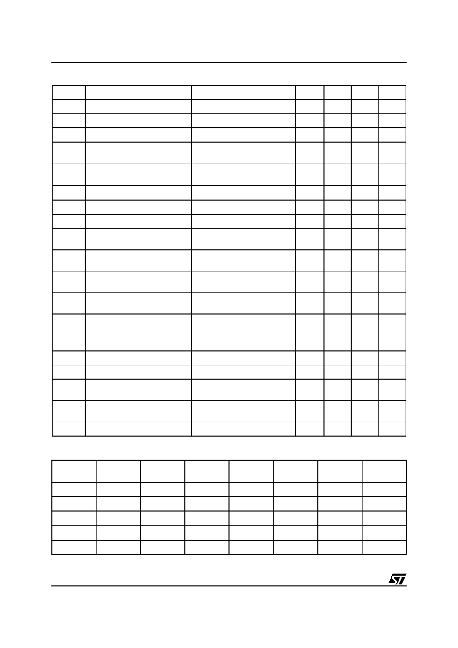
STA510
4/7
LOGIC TRUTH TABLE (see fig. 2)
t
r
Rise time
Resistive load;
50
ns
t
f
Fall time
Resistive load;
50
ns
V
CC
Supply voltage operating range
11
55
V
V
IN-H
High level input voltage
V
Ibias
/2
+150mV
V
Ibias
/2
+300mV
V
V
IN-L
Low level input voltage
V
Ibias
/2
-300mV
V
Ibias
/2
-130mV
V
I
IN-H
Hi level Input current
Pin voltage = V
Ibias
1
µ
A
I
IN-L
Low level input current
Pin voltage = 0.3V
1
µ
A
I
PWRDN-H
Hi level PWRDN pin input current
Ibias = 3.3V
35
µ
A
V
L
Low logical state voltage (pin
PWRDN, TRISTATE)
Ibias = 3.3V
0.8
1
V
V
H
High logical state voltage (pin
PWRDN, TRISTATE)
Ibias = 3.3V
1.9
2.2
V
I
VCC-
PWRDN
Supply current from Vcc in Power
Down
PWRDN = 0; TRISTATE = 0
0.25
mA
I
VCC-hiz
Supply current from Vcc in Tri-
state
PWRDN = 1; Tri-state=0;
TBD
mA
I
VCC
Supply current from Vcc in
operation
No LOAD
Input pulse width = 50% Duty;
Switching Frequency = 384Khz;
No LC filters;
100
mA
I
lim
Current Limit (Overload)
6
7
8
A
I
sc
Short circuit current threshold
7
8
9
A
V
UV
Undervoltage protection threshold
on VREG
7
V
V
OV
Overvoltage protection threshold
on VCC
55
60
V
V
DROP
Dropout from VCC to VREG
4
V
TRI-STATE
INL
INR
HSL (Q1)
HSR (Q2)
LSL (Q3)
LSR (Q4)
OUTPUT
MODE
0
x
x
OFF
OFF
OFF
OFF
Hi-Z
1
0
0
OFF
OFF
ON
ON
DUMP
1
0
1
OFF
ON
ON
OFF
NEGATIVE
1
1
0
ON
OFF
OFF
ON
POSITIVE
1
1
1
ON
ON
OFF
OFF
Not used
Symbol
Parameter
Test conditions
Min.
Typ.
Max.
Unit
ELECTRICAL CHARACTERISTCS (continued)
5/7
STA510
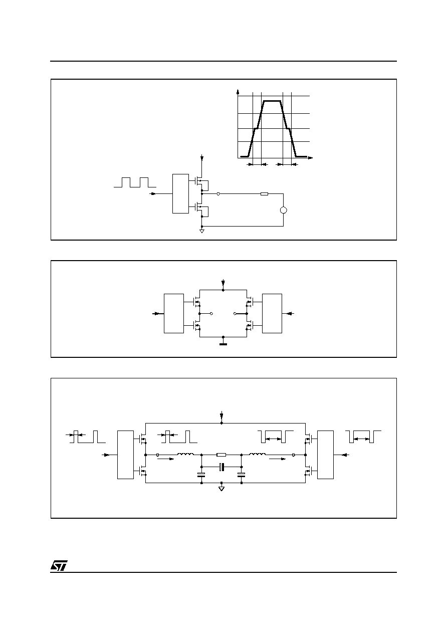
Figure 1. Test Circuit.
Figure 2.
Figure 3.
D
t_s
= Low current dead time = MAX(DTr,DTf)
OUTx
Vcc
(3/4)Vcc
(1/2)Vcc
(1/4)Vcc
t
DTf
DTr
Duty cycle = 50%
INx
OUTx
gnd
+Vcc
R 8
+
-
vdc = Vcc/2
D03AU1507
INL
INR
+V
CC
Q1
Q3
Q2
Q4
OUTL
GND
OUTR
D03AU1456
D
t_d
= High Current Dead time for Bridge application = ABS(DTout(L)-DTin(L))+ABS(DTOUT(R)-DTin(R))
+V
CC
Rload=8
Q2
OUTR
DTout(R)
DTin(R)
DTout(L)
470nF
470nF
470nF
Iout=5A
Iout=5A
Q4
Q1
Q3
INR
D03AU1457
INL
DTin(A)
Duty cycle=A
Duty cycle=B
Duty cycle A and B: Fixed to have DC output current of 5A in the direction shown in figure
22
µ
H
22
µ
H
OUTL