 | –≠–ª–µ–∫—Ç—Ä–æ–Ω–Ω—ã–π –∫–æ–º–ø–æ–Ω–µ–Ω—Ç: STA530 | –°–∫–∞—á–∞—Ç—å:  PDF PDF  ZIP ZIP |
1/17
STA530
July 2003
s
MONOCHIP BRIDGE QUAD CONFIGURABLE
AMPLIFIER OPTIMIZED FOR BASH
Æ
ARCHITECTURE
s
4 X 50W OUTPUT POWER @ R
L
= 8
,
THD = 10% or (2 x 50W @ 8
+ 1 x 100W @
4
) or (2 x 100W @ 4
)
s
PRECISION RECTIFIERS TO DRIVE THE
BUCK REGULATOR
s
ON-OFF SEQUENCE/ TIMER WITH MUTE
AND STANDBY
s
PROPORTIONAL OVER POWER OUTPUT
CURRENT TO LIMIT THE BUCK REGULATOR
s
ABSOLUTE POWER BRIDGE OUTPUT
TRANSISTOR POWER PROTECTION
s
ABSOLUTE OUTPUT CURRENT LIMIT
s
INTEGRATED THERMAL PROTECTION
s
POWER SUPPLY OVER VOLTAGE
PROTECTION
s
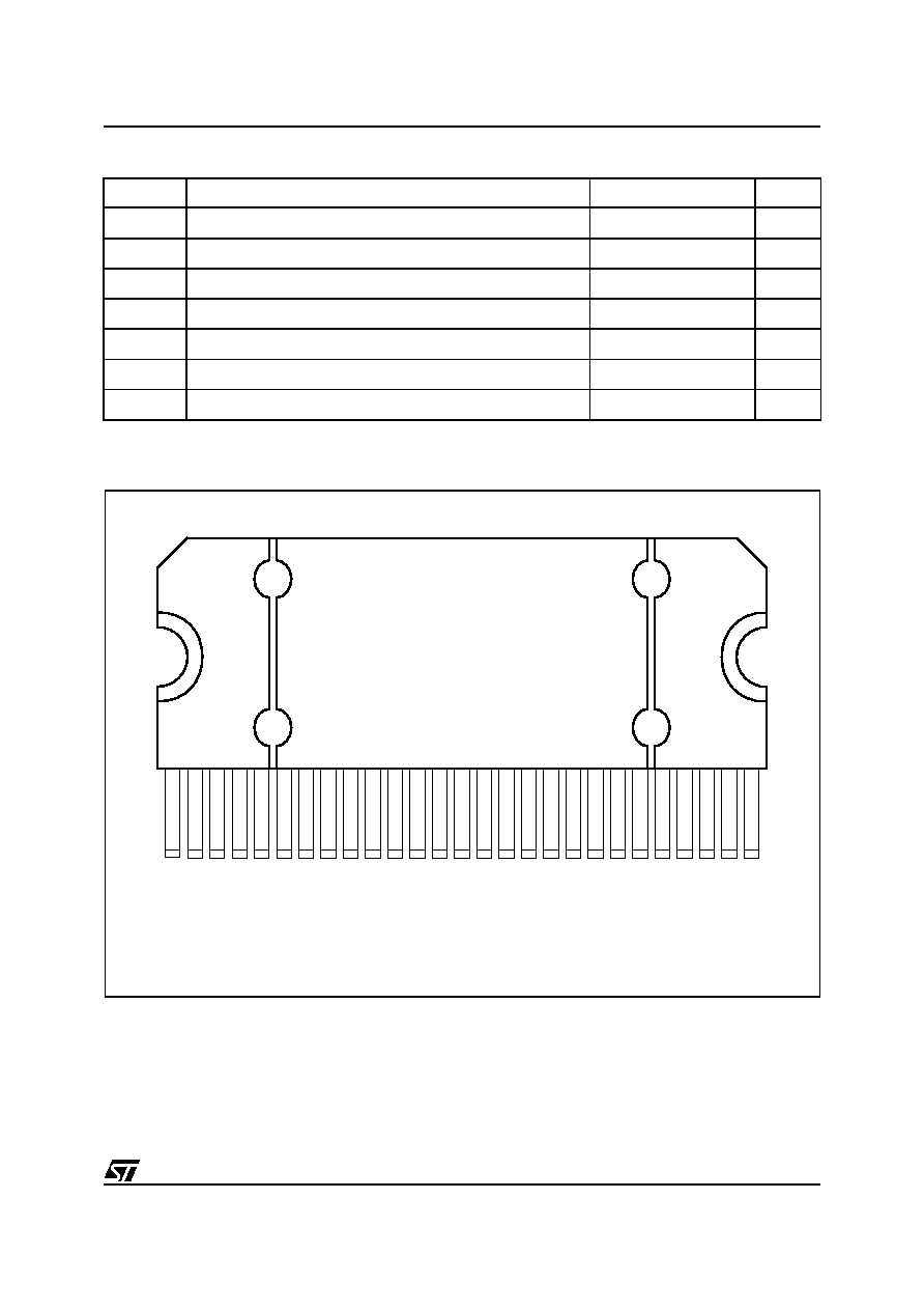
FLEXIWATT POWER PACKAGE WITH 27 PIN
s
BASHÆ LICENCE REQUIRED
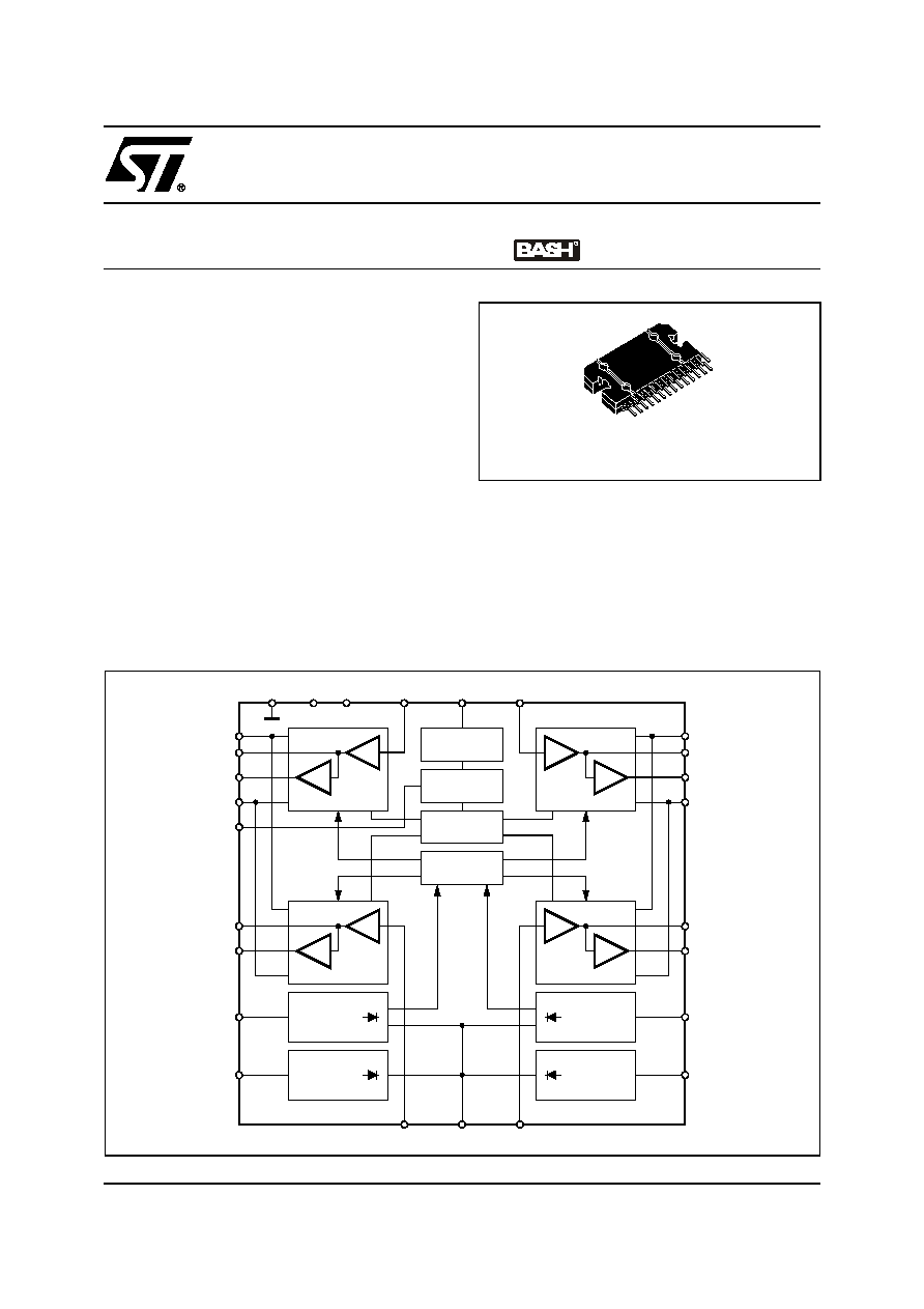
DESCRIPTION
The STA530 is a BASH
Æ
power amplifier where
BASH
Æ
means "High Efficiency".
FLEXIWATT27
4 X 50W STEREO
POWER AMPLIFIER
BLOCK DIAGRAM
OUTPUT BRIDGE
TURN-ON/OFF
SEQUENCE
ABSOLUTE
VALUE
BLOCK
PROTECTION
+10
-1
SOA
DETECTOR
CONFIG.
OUTPUT BRIDGE
+10
-1
ABSOLUTE
VALUE
BLOCK
CD+1&2
OUT1+
OUT1-
CD-1&2
PROT
OUT2+
OUT2-
TRK_2/PAR1&2
TRK_1
OUTPUT BRIDGE
ABSOLUTE
VALUE
BLOCK
+10
-1
OUTPUT BRIDGE
+10
-1
ABSOLUTE
VALUE
BLOCK
CD+3&4
OUT3+
OUT3-
CD-3&4
OUT4+
OUT4-
TRK_4/PAR3&4
TRK_3
PWR_INP1
GND
+V
S
-V
S
STBY/MUTE
PWR_INP2
PWR_INP3
PWR_INP4
TRK_OUT
D02AU1344
STA530
2/17
DESCRIPTION (continued)
In fact it's permits to build a BASHÆ architecture amplifier adding only few external components and a variable
Buck regulator tracking the audio signal. Notice that normally only one Buck regulator is used to supply a mul-
tichannel amplifiers system , therefore most of the functions implemented in the circuit have a summing output
pin.
The signal circuits are biased by fixed negative and positive voltages referred to Ground. Instead the final stag-
es of the output amplifiers are supplied by two external voltages that are following the audio signal . In this way
the headroom for the output transistors is kept at minimum level to obtain a high efficiency power amplifier.
The circuit contains all the blocks to build a configurable four channel amplifier.
The tracking signal for the external Buck regulator is generated from the Absolute Value Block (AVB) that rec-
tifies the audio signal. The outputs of these blocks are decoupled by a diode to permit an easy sum of this signal
for the multichannel application. The gain of the stage AVB is equal to 70 (+36.9 dB). A sophisticated circuit
performs the output transistor power detector that , with the buck regulator, reduces the power supply voltage .
Moreover, a maximum current output limiting and the over temperature sensor have been added to protect the
circuit itself. The external voltage applied to the STBY/MUTE pin forces the two amplifiers in the proper condi-
tion to guarantee a silent turn-on and turn-off.
ABSOLUTE MAXIMUM RATINGS
Notes: 1. V
CD-
must not be more negative than -Vs
THERMAL DATA
Symbol
Parameter
Value
Unit
+V
s
Positive supply voltage referred to pin 14 (GND)
27
V
-V
s
Negative supply voltage referred to pin 14 (GND)
-27
V
V
CD+
Positive supply voltage tracking rail referred to pin 14 (GND)
20
V
V
CD-
Negative supply voltage referred to -Vs
(1)
-0.3
V
V
CD-
Negative supply voltage tracking rail referred to pin 14 (GND)
-20
V
V
PWR_Imp1
V
PWR_Imp2
V
TRK_1
V
TRK_2
Pin 11, 10, 9, 8 Negative & Positive maximum voltage referred to
GND (pin 14)
-25 to +25
V
V
PWR_Imp 3
V
PWR_Imp 4
V
TRK_3
V
TRK_4
Pin 17, 18, 19, 20 Negative & Positive maximum voltage referred
to GND (pin 14)
-25 to +25
V
I
STBY-max
Pin 12 maximum input current (Internal voltage clamp at 5V)
500
µ
A
V
STBY/
MUTE
Pin 12 negative maximum voltage referred to GND (pin 14)
-0.5
V
Symbol
Parameter
Value
Unit
T
j
Max Junction temperature
150
∞C
R
th j_case
Thermal Resistance Junction to case
.............................. ..
max
1
∞
C/W
3/17
STA530
OPERATING RANGE
PIN CONNECTION
NOTE
Slug connected to PINs No. 1 & 27
Symbol
Parameter
Value
Unit
+V
s
Positive supply voltage
+15 to +25
V
-V
s
Negative supply voltage
-15 to -25
V
V
s+
Delta positive supply voltage
5V
(Vs+ - VCD+)
10V
V
V
CD+
Positive supply voltage tracking rail
+3 to +15
V
V
CD-
Negative supply voltage tracking rail
-15 to -3
V
T
amb
Ambient Temperature Range
0 to 70
∞C
I
sb_max
Pin 12 maximum input current (Internal voltage clamp at 5V)
200
µ
A
D02AU1352
Out1+
-Vs
Out1-
CD+1&2
CD-1&2
Out2-
Out2+
TRK_2/Par1&2
TRK_1
PWR_Inp2
PWR_Inp1
STBY/MUTE
TRK_Out
Gnd
+Vs
PROT
PWR_Inp3
PWR_Inp4
TRK_3
TRK_4/Par3&4
Out4+
Out4-
CD-3&4
CD+3&4
Out3-
Out3+
-Vs
1
27

STA530
4/17
PIN CONNECTION
N∞
Name
Description
1
-Vs
Negative Bias Supply
2
Out1+
Channel 1 speaker positive output
3
Out1-
Channel 1 speaker negative output
4
CD+1&2
Channels 1 & 2 Time varying tracking rail positive power supply
5
CD-1&2
Channels 1 &2 Time varying tracking rail negative power supply
6
Out2-
Channel 2 speaker negative output
7
Out2+
Channel 2 speaker positive output
8
TRK_2/
Par1&2
Absolute value block input for channel 2,and parallel command for channels 1&2
9
TRK_1
Absolute value block input for channel 1
10
PWR_Inp2
Input to channel 2 power stage
11
PWR_Inp1
Input to channel 1 power stage
12
STBY/MUTE
Standby/mute input voltage control
13
TRK_Out
Absolute value block output
14
Gnd
Analog Ground
15
+Vs
Positive Bias Supply
16
PROT
Channel Protection signal for STABP01
17
PWR_Inp3
Input to channel 3 power stage
18
PWR_Inp4
Input to channel 4 power stage
19
TRK_3
Absolute value block input for channel 3
20
TRK_4/
Par3&4
Absolute value block input for channel 4,and parallel command for channels 3&4
21
Out4+
Channel 4 speaker positive output
22
Out4-
Channel 4 speaker negative output
23
CD-3&4
Channels 3 & 4 Time varying tracking rail negative power supply
24
CD+3&4
Channels 3 & 4 Time varying tracking rail positive power supply
25
Out3-
Channel 3 speaker negative output
26
Out3+
Channel 3 speaker positive output
27
-Vs
Negative Bias Supply
5/17
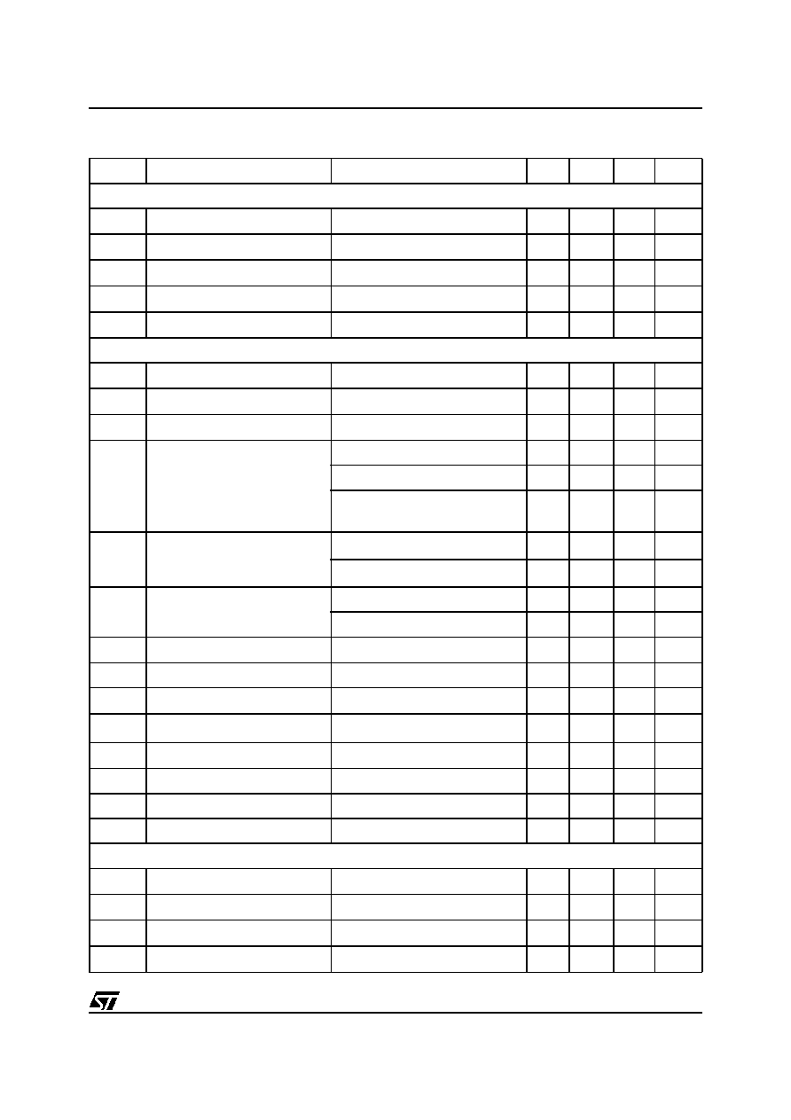
STA530
ELECTRICAL CHARACTERISTCS (Test Condition: Vs+ = 25V, Vs- = -25V, V
CD+
= 15V, V
CD-
= -15V, R
L
=
8
, external components at the nominal value f = 1KHz, Tamb = 25∞C unless otherwise specified)
Symbol
Parameter
Test Condition
Min.
Typ.
Max.
Unit
TRACKING PARAMETERS
G
TRK
Tracking reference voltage gain
66
70
74
V
TRK_out
Tracking ref. output voltage
0
15
V
I
TRK_out
Current capability
5
6
mA
Z
TRK_in
Input impedance (T
RK1/2
)
1
M
V
OFFSET
Output traking DC offset
100
mV
OUTPUT BRIDGE
G
out
Half Output bridge gain
19
20
21
dB
G
ch
Output bridge differential gain
25
26
27
dB
G
ch
Output bridges gain mismatch
-1
1
dB
P
out
Continuous Output Power
THD = 1%
39
W
THD = 10%
50
W
THD = 10% R
L
= 4
V
CD+
= 11V, V
CD-
= -11V
40
W
P
out
2 ch par
Continuous Output Power
THD = 1% R
L
= 4
78
W
THD = 10% R
L
= 4
100
W
THD
Total harmonic distortion of the
output bridge
Po = 5W
0.01
0.1
%
f = 20Hz to 20KHz; Po = 20W
0.2
%
V
Off
Output bridge D.C. offset
-100
100
mV
EN
Noise at Output bridge pins
f = 20Hz to 20KHz; Rg = 50
60
µ
V
Z
br_in
Input impedance
100
140
180
K
R
dson
Output power Rdson
I
O
= 1A
Tj=25
o
C
400
500
m
R
dsonMAX
Maximum Output power Rdson
I
O
= 1A
800
m
OLG
Open Loop Voltage Gain
100
dB
GB
Unity Gain Bandwidth
6
MHz
SR
Slew Rate
8
V/
µ
s
PROTECTION
V
STBY
Stby voltage range
0
0.8
V
V
MUTE
Mute voltage range
1.6
2.5
V
V
PLAY
Play voltage range
4
5
V
T
h1
First Over temperature threshold
130
∞C