
1/12
February 2005
STP130NS04ZB
STB130NS04ZB - STW130NS04ZB
N-CHANNEL CLAMPED - 7 m
- 80A TO-220/D≤PAK/TO-247
FULLY PROTECTED MESH OVERLAYTM MOSFET
Table 1: General Features
s
TYPICAL R
DS
(on) = 7 m
s
100% AVALANCHE TESTED
s
LOW CAPACITANCE AND GATE CHARGE
s
175∞C MAXIMUM JUNCTION TEMPERATURE
DESCRIPTION
This fully clamped MOSFET is produced by using
the latest advanced Company's Mesh Overlay
process which is based on a novel strip layout.
The inherent benefits of the new technology cou-
pled with the extra clamping capabilities make this
product particularly suitable for the harshest oper-
ation conditions such as those encountered in the
automotive environment .Any other application re-
quiring extra ruggedness is also recommended.
APPLICATIONS
s
HIGH SWITCHING CURRENT
s
LINEAR APPLICATIONS
Table 2: Order Codes
Figure 1: Package
Figure 2: Internal Schematic Diagram
TYPE
V
DSS
R
DS(on)
I
D
STP130NS04ZB
STB130NS04ZB
STW130NS04ZB
CLAMPED
CLAMPED
CLAMPED
< 9 m
< 9 m
< 9 m
80 A
80 A
80 A
1
2
3
TO-220
D≤PAK
1
3
1
2
3
TO-247
Sales Type
Marking
Package
Packaging
STP130NS04ZB
P130NS04ZB
TO-220
TUBE
STB130NS04ZBT4
B130NS04ZB
D≤PAK
TAPE & REEL
STW130NS04ZB
W130NS04ZB
TO-247
TUBE
Rev. 2
STP130NS04ZB - STB130NS04ZB - STW130NS04ZB
2/12
Table 3: Absolute Maximum ratings
( ) Pulse width limited by safe operating area
Table 4: Thermal Data
(*)When mounted on 1 inch≤ FR4 2oZ Cu
Table 5: Avalanche Characteristics
Symbol
Parameter
Value
Unit
V
DS
Drain-source Voltage (V
GS
= 0)
CLAMPED
V
V
DG
Drain-gate Voltage
CLAMPED
V
V
GS
Gate- source Voltage
CLAMPED
V
I
D
Drain Current (continuous) at T
C
= 25∞C
80
A
I
D
Drain Current (continuous) at T
C
= 100∞C
60
A
I
DG
Drain Gate Current (continuous)
±
50
mA
I
GS
Gate Source Current (continuous)
±
50
mA
I
DM
( )
Drain Current (pulsed)
320
A
P
TOT
Total Dissipation at T
C
= 25∞C
300
W
Derating Factor
2.0
W/∞C
V
ESD(G-S)
Gate-Source ESD(HBM-C=100 pF, R=1.5 K
)
4
KV
T
j
T
stg
Max Operating Junction Temperature
Storage Temperature
-55 to 175
∞C
TO-220
D≤PAK
TO-247
Unit
Rthj-case
Thermal Resistance Junction-case Max
0.50
∞C/W
Rthj-pcb (*)
Thermal Resistance Junction-pcb Max
--
35
--
∞C/W
Rthj-a
Thermal Resistance Junction-ambient Max
62.5
--
50
T
l
Maximum Lead Temperature For Soldering
Purpose (1.6 mm from case, for 10 sec)
300
∞C
Symbol
Parameter
Max Value
Unit
I
AR
Avalanche Current, Repetitive or Not-Repetitive
(pulse width limited by T
j
max)
80
A
E
AS
Single Pulse Avalanche Energy
(starting T
j
= 25 ∞C, I
D
= I
AR
, V
DD
= 30 V)
500
mJ
3/12
STP130NS04ZB - STB130NS04ZB - STW130NS04ZB
ELECTRICAL CHARACTERISTICS (T
CASE
=25∞C UNLESS OTHERWISE SPECIFIED)
Table 6: On/Off
Table 7: Dynamic
Table 8: Source Drain Diode
(1) Pulsed: Pulse duration = 300 µs, duty cycle 1.5 %.
(2) Pulse width limited by safe operating area.
Symbol
Parameter
Test Conditions
Min.
Typ.
Max.
Unit
V
(BR)DSS
Clamped Voltage
I
D
= 1 mA, V
GS
= 0
-40 < Tj < 175 ∞C
33
V
I
DSS
Zero Gate Voltage
Drain Current (V
GS
= 0)
V
DS
= 16 V,Tj = 25 ∞C
V
DS
= 16 V,Tj = 125 ∞C
10
100
µA
µA
I
GSS
Gate-body Leakage
Current (V
DS
= 0)
V
GS
= ±10 V,Tj = 25 ∞C
10
µA
V
GSS
Gate-Source
Breakdown Voltage
I
GS
= ±100 µA
18
V
V
GS(th)
Gate Threshold Voltage
V
DS
= V
GS
= I
D
= 1 mA
2
4
V
R
DS(on)
Static Drain-source On
Resistance
V
GS
= 10 V ,I
D
= 40 A
7
9
m
Symbol
Parameter
Test Conditions
Min.
Typ.
Max.
Unit
g
fs
Forward
Transconductance
V
DS
= 15 V, I
D
= 40 A
50
S
C
iss
C
oss
C
rss
Input Capacitance
Output Capacitance
Reverse Transfer
Capacitance
V
DS
= 25 V, f = 1MHz, V
GS
= 0
2700
1275
285
pF
pF
pF
t
d(on)
t
f
t
d(off)
t
f
Turn-on Delay Time
Fall Time
Turn-off Delay Time
Fall Time
V
DD
= 17.5 V, I
D
= 40 A,
R
G
= 4.7
,
V
GS
= 10 V
(see Figure 15)
40
220
170
100
ns
ns
ns
ns
Q
g
Q
gs
Q
gd
Total Gate Charge
Gate-Source Charge
Gate-Drain Charge
V
DD
= 20 V, I
D
= 80 A,
V
GS
= 10 V
(see Figure 17)
80
20
27
105
nC
nC
nC
Symbol
Parameter
Test Conditions
Min.
Typ.
Max.
Unit
I
SD
I
SDM
(2)
Source-drain Current
Source-drain Current (pulsed)
80
320
A
A
V
SD
(1)
Forward On Voltage
I
SD
= 80 A, V
GS
= 0
1.5
V
t
rr
Q
rr
I
RRM
Reverse Recovery Time
Reverse Recovery Charge
Reverse Recovery Current
I
SD
= 80 A, di/dt = 100A/µs
V
DD
= 25V, T
j
= 150∞C
(see Figure 16)
90
0.18
4
ns
µC
A
STP130NS04ZB - STB130NS04ZB - STW130NS04ZB
4/12
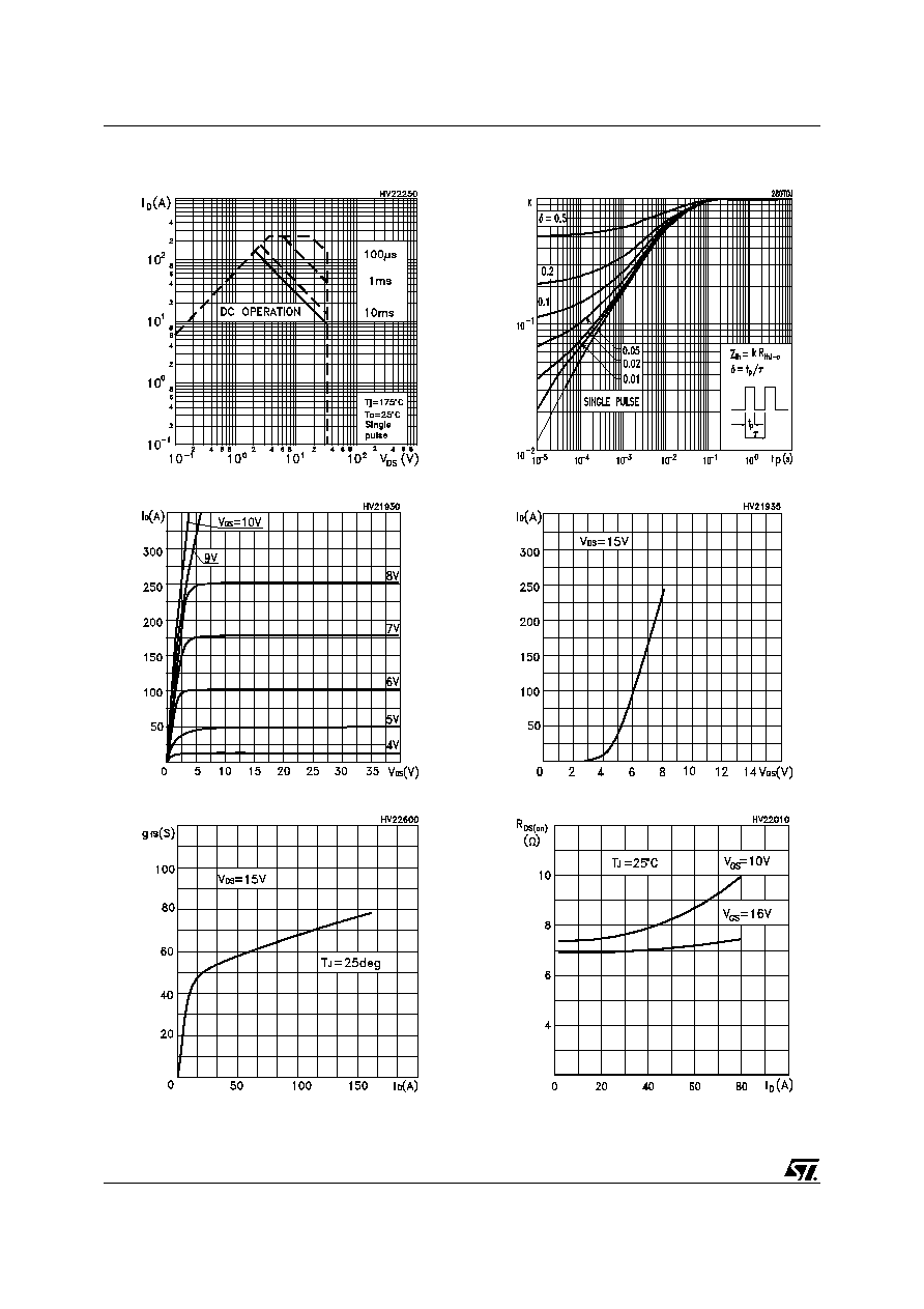
Figure 3: Safe Operating Area
Figure 4: Output Characteristics
Figure 5: Transconductance
Figure 6: Thermal Impedance
Figure 7: Transfer Characteristics
Figure 8: Static Drain-source On Resistance
5/12
STP130NS04ZB - STB130NS04ZB - STW130NS04ZB
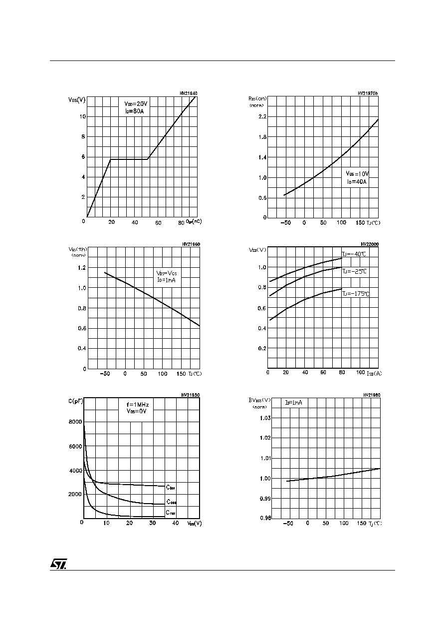
Figure 9: Gate Charge vs Gate-source Voltage
Figure 10: Normalized Gate Thereshold Volt-
age vs Temperature
Figure 11: Capacitance Variations
Figure 12: Normalized On Resistance vs Tem-
perature
Figure 13: Source-drain Diode Forward Char-
acteristics
Figure 14: Normalized BVDSS vs Temperature
STP130NS04ZB - STB130NS04ZB - STW130NS04ZB
6/12
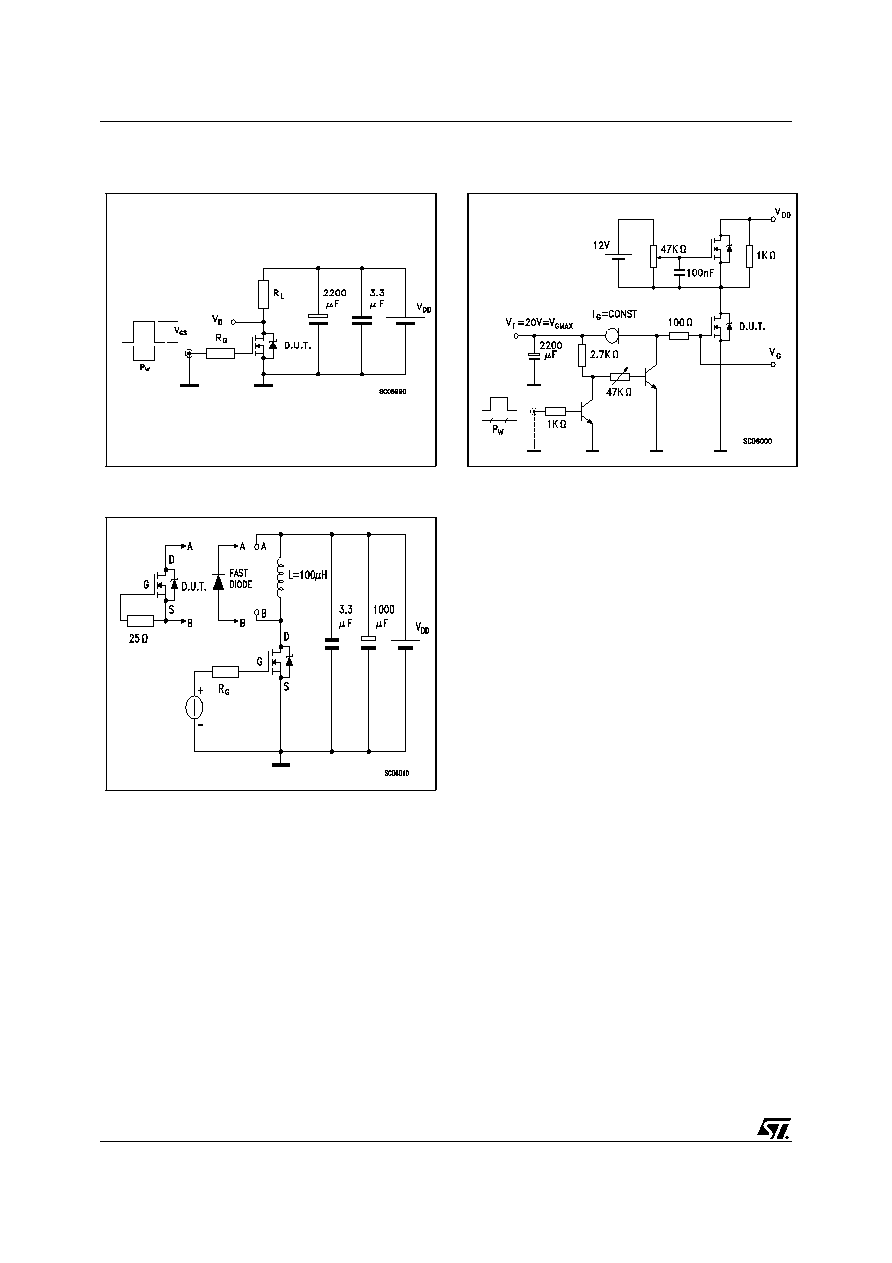
Figure 15: Switching Times Test Circuit For
Resistive Load
Figure 16: Test Circuit For Diode Recovery Be-
haviour
Figure 17: Gate Charge Test Circuit
7/12
STP130NS04ZB - STB130NS04ZB - STW130NS04ZB
DIM.
mm.
inch
MIN.
TYP
MAX.
MIN.
TYP.
MAX.
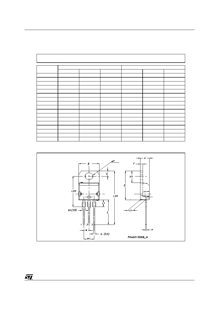
A
4.40
4.60
0.173
0.181
b
0.61
0.88
0.024
0.034
b1
1.15
1.70
0.045
0.066
c
0.49
0.70
0.019
0.027
D
15.25
15.75
0.60
0.620
E
10
10.40
0.393
0.409
e
2.40
2.70
0.094
0.106
e1
4.95
5.15
0.194
0.202
F
1.23
1.32
0.048
0.052
H1
6.20
6.60
0.244
0.256
J1
2.40
2.72
0.094
0.107
L
13
14
0.511
0.551
L1
3.50
3.93
0.137
0.154
L20
16.40
0.645
L30
28.90
1.137
¯P
3.75
3.85
0.147
0.151
Q
2.65
2.95
0.104
0.116
TO-220 MECHANICAL DATA
STP130NS04ZB - STB130NS04ZB - STW130NS04ZB
8/12
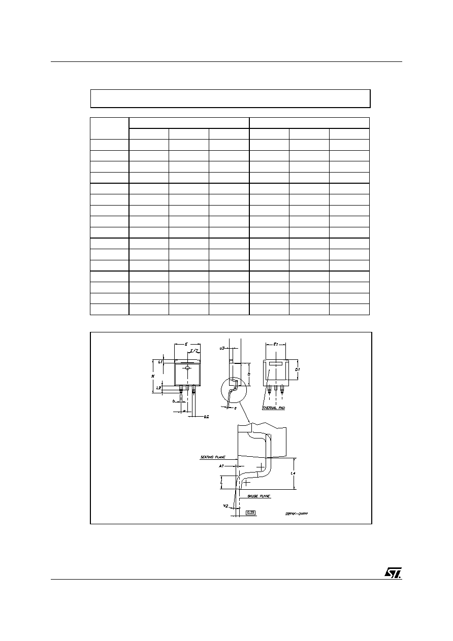
DIM.
mm.
inch
MIN.
TYP
MAX.
MIN.
TYP.
MAX.
A
4.32
4.57
0.178
0.180
A1
0.00
0.25
0.00
0.009
b
0.71
0.91
0.028
0.350
b2
1.15
1.40
0.045
0.055
c
0.46
0.61
0.018
0.024
c2
1.22
1.40
0.048
0.055
D
8.89
9.02
9.40
0.350
0.355
0.370
D1
8.01
0.315
E
10.04
10.28
0.395
0.404
e
2.54
0.010
H
13.10
13.70
0.515
0.540
L
1.30
1.70
0.051
0.067
L1
1.15
1.39
0.045
0.054
L2
1.27
1.77
0.050
0.069
L4
2.70
3.10
0.106
0.122
V2
0∞
8∞
0∞
8∞
TO-263 (D
2
PAK) MECHANICAL DATA
9/12
STP130NS04ZB - STB130NS04ZB - STW130NS04ZB
DIM.
mm.
inch
MIN.
TYP
MAX.
MIN.
TYP.
MAX.
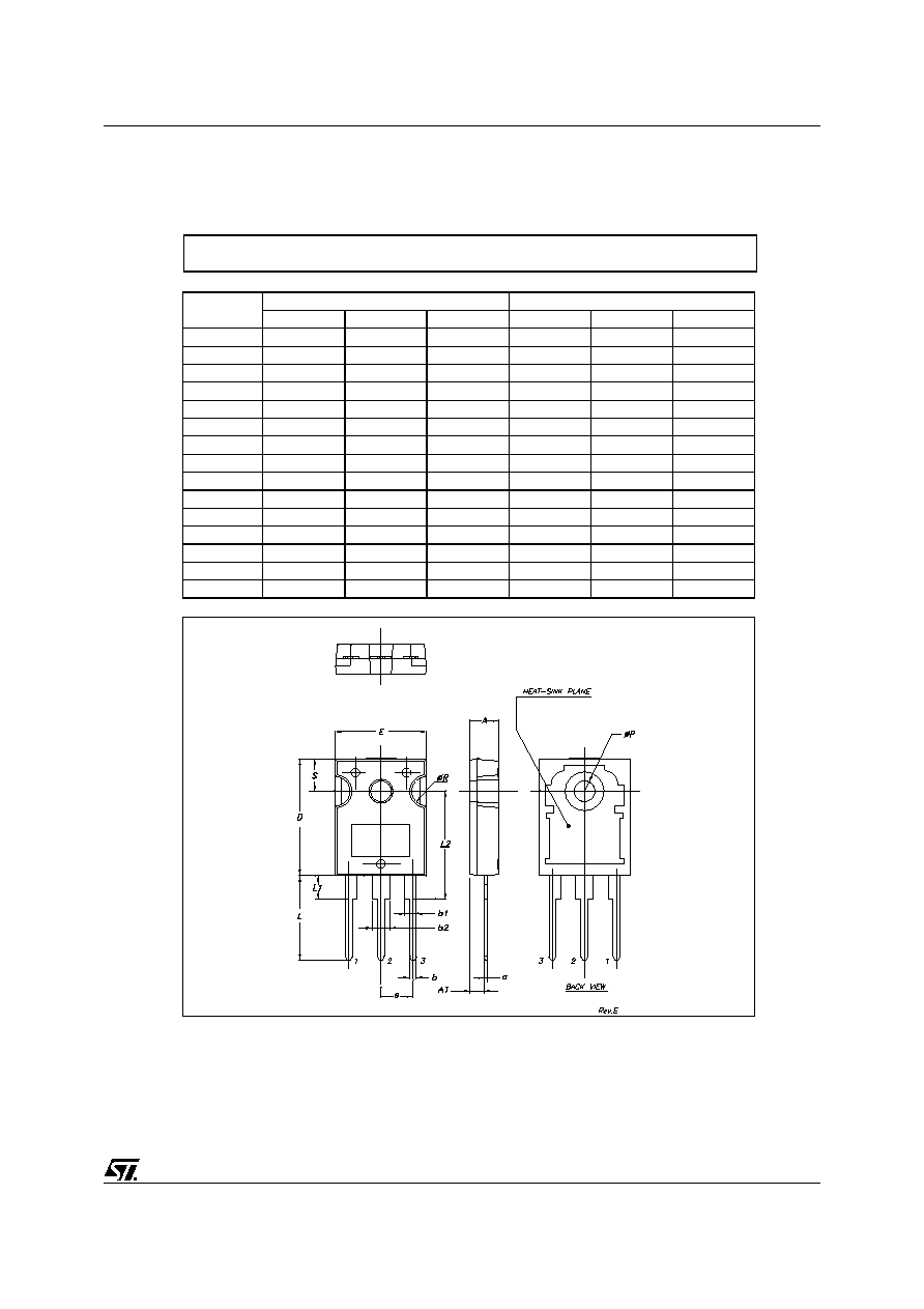
A
4.85
5.15
0.19
0.20
A1
2.20
2.60
0.086
0.102
b
1.0
1.40
0.039
0.055
b1
2.0
2.40
0.079
0.094
b2
3.0
3.40
0.118
0.134
c
0.40
0.80
0.015
0.03
D
19.85
20.15
0.781
0.793
E
15.45
15.75
0.608
0.620
e
5.45
0.214
L
14.20
14.80
0.560
0.582
L1
3.70
4.30
0.14
0.17
L2
18.50
0.728
¯P
3.55
3.65
0.140
0.143
¯R
4.50
5.50
0.177
0.216
S
5.50
0.216
TO-247 MECHANICAL DATA
STP130NS04ZB - STB130NS04ZB - STW130NS04ZB
10/12
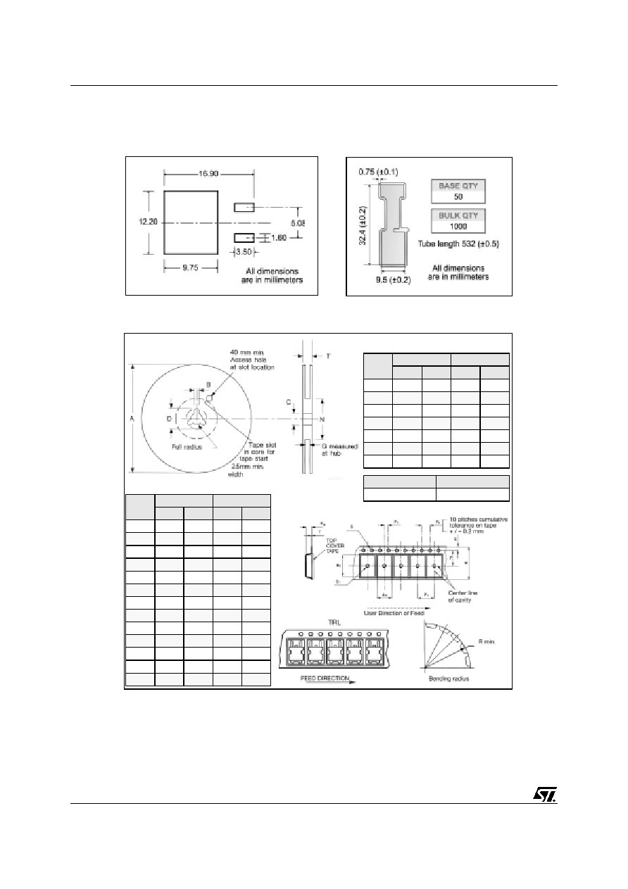
TAPE AND REEL SHIPMENT (suffix "T4")*
TUBE SHIPMENT (no suffix)*
D
2
PAK FOOTPRINT
* on sales type
DIM.
mm
inch
MIN.
MAX.
MIN.
MAX.
A
330
12.992
B
1.5
0.059
C
12.8
13.2
0.504
0.520
D
20.2
0795
G
24.4
26.4
0.960
1.039
N
100
3.937
T
30.4
1.197
BASE QTY
BULK QTY
1000
1000
REEL MECHANICAL DATA
DIM.
mm
inch
MIN.
MAX.
MIN.
MAX.
A0
10.5
10.7
0.413
0.421
B0
15.7
15.9
0.618
0.626
D
1.5
1.6
0.059
0.063
D1
1.59
1.61
0.062
0.063
E
1.65
1.85
0.065
0.073
F
11.4
11.6
0.449
0.456
K0
4.8
5.0
0.189
0.197
P0
3.9
4.1
0.153
0.161
P1
11.9
12.1
0.468
0.476
P2
1.9
2.1
0.075
0.082
R
50
1.574
T
0.25
0.35
0.0098 0.0137
W
23.7
24.3
0.933
0.956
TAPE MECHANICAL DATA

11/12
STP130NS04ZB - STB130NS04ZB - STW130NS04ZB
Table 9: Revision History
Date
Revision
Description of Changes
10-June-2004
1
First Release.
14-Jan-2005
2
Inserted D≤PAK, Complete version.

STP130NS04ZB - STB130NS04ZB - STW130NS04ZB
12/12
Information furnished is believed to be accurate and reliable. However, STMicroelectronics assumes no responsibility for the consequences
of use of such information nor for any infringement of patents or other rights of third parties which may result from its use. No license is granted
by implication or otherwise under any patent or patent rights of STMicroelectronics. Specifications mentioned in this publication are subject
to change without notice. This publication supersedes and replaces all information previously supplied. STMicroelectronics products are not
authorized for use as critical components in life support devices or systems without express written approval of STMicroelectronics.
The ST logo is a registered trademark of STMicroelectronics
All other names are the property of their respective owners
© 2005 STMicroelectronics - All Rights Reserved
STMicroelectronics group of companies
Australia - Belgium - Brazil - Canada - China - Czech Republic - Finland - France - Germany - Hong Kong - India - Israel - Italy - Japan -
Malaysia - Malta - Morocco - Singapore - Spain - Sweden - Switzerland - United Kingdom - United States of America