1/7
PRELIMINARY DATA
May 2002
This is preliminary information on a new product now in development or undergoing evaluation. Details are subject to change without notice.
STB160NF3LL
N-CHANNEL 30V - 0.0026
- 160A D
2
PAK
STripFETTM II POWER MOSFET
s
TYPICAL R
DS
(on) = 0.0026
s
LOW THRESHOLD DRIVE
s
ULTRA LOW ON-RESISTANCE
s
LOGIC LEVEL DEVICE
s
100% AVALANCHE TESTED
s
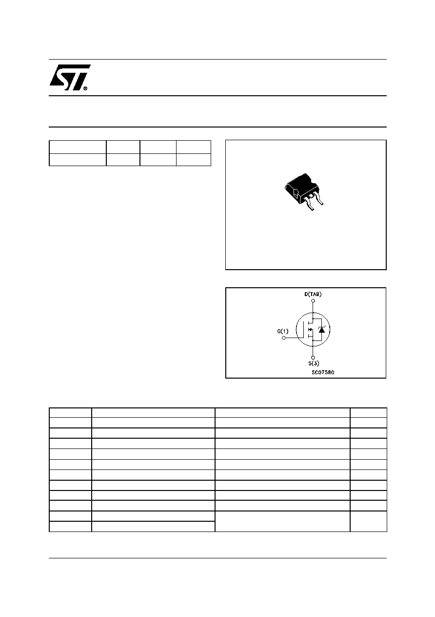
SURFACE-MOUNTING D
2
PAK (TO-263)
POWER PACKAGE IN TUBE (NO SUFFIX) OR
IN TAPE & REEL (SUFFIX "T4")
DESCRIPTION
This Power MOSFET is the latest development of
STMicroelectronis unique "Single Feature SizeTM"
strip-based process. The resulting transistor
shows extremely high packing density for low on-
resistance, rugged avalanche characteristics and
less critical alignment steps therefore a remark-
able manufacturing reproducibility.
APPLICATIONS
s
HIGH CURRENT, HIGH SWITCHING SPEED
s
MOTOR CONTROL, AUDIO AMPLIFIERS
s
DC-DC & DC-AC CONVERTERS
s
SOLENOID AND RELAY DRIVERS
TYPE
V
DSS
R
DS(on)
I
D
ST160NF3LL
30 V
<0.003
160 A
1
3
D
2
PAK
TO-263
(Suffix "T4")
ABSOLUTE MAXIMUM RATINGS
(
∑)
Pulse width limited by safe operating area.
(*) Current Limited by Package
(1) Starting T
j
= 25
o
C, I
D
= 80A, V
DD
= 20V
Symbol
Parameter
Value
Unit
V
DS
Drain-source Voltage (V
GS
= 0)
30
V
V
DGR
Drain-gate Voltage (R
GS
= 20 k
)
30
V
V
GS
Gate- source Voltage
± 15
V
I
D
(
)
Drain Current (continuous) at T
C
= 25∞C
160
A
I
D
Drain Current (continuous) at T
C
= 100∞C
160
A
I
DM
(
∑)
Drain Current (pulsed)
640
A
P
tot
Total Dissipation at T
C
= 25∞C
300
W
Derating Factor
2
W/∞C
E
AS
(1)
Single Pulse Avalanche Energy
1.2
J
T
stg
Storage Temperature
-55 to 175
∞C
T
j
Max. Operating Junction Temperature
INTERNAL SCHEMATIC DIAGRAM
STB160NF3LL
2/7
THERMAL DATA
ELECTRICAL CHARACTERISTICS (T
case
= 25 ∞C unless otherwise specified)
OFF
ON
(*)
DYNAMIC
Rthj-case
Rthj-amb
T
l
Thermal Resistance Junction-case
Thermal Resistance Junction-ambient
Maximum Lead Temperature For Soldering Purpose
Max
Max
0.5
62.5
300
∞C/W
∞C/W
∞C
Symbol
Parameter
Test Conditions
Min.
Typ.
Max.
Unit
V
(BR)DSS
Drain-source
Breakdown Voltage
I
D
= 250 µA
V
GS
= 0
30
V
I
DSS
Zero Gate Voltage
Drain Current (V
GS
= 0)
V
DS
= Max Rating
V
DS
= Max Rating T
C
= 125∞C
1
10
µA
µA
I
GSS
Gate-body Leakage
Current (V
DS
= 0)
V
GS
= ± 15 V
±100
nA
Symbol
Parameter
Test Conditions
Min.
Typ.
Max.
Unit
V
GS(th)
Gate Threshold Voltage
V
DS
= V
GS
I
D
= 250
µ
A
1
V
R
DS(on)
Static Drain-source On
Resistance
V
GS
= 10 V
I
D
= 80 A
V
GS
= 4.5 V
I
D
= 80 A
0.0026
0.0032
0.0030
0.0043
Symbol
Parameter
Test Conditions
Min.
Typ.
Max.
Unit
g
fs
(*)
Forward Transconductance
V
DS
= 15 V
I
D
=80 A
60
S
C
iss
C
oss
C
rss
Input Capacitance
Output Capacitance
Reverse Transfer
Capacitance
V
DS
= 25V f = 1 MHz V
GS
= 0
6200
1720
300
pF
pF
pF
3/7
STB160NF3LL
SWITCHING ON
(*)
SWITCHING OFF
(*)
SOURCE DRAIN DIODE
(*)
(*)
Pulsed: Pulse duration = 300 µs, duty cycle 1.5 %.
(
∑)
Pulse width limited by T
jmax
Symbol
Parameter
Test Conditions
Min.
Typ.
Max.
Unit
t
d(on)
t
r
Turn-on Time
Rise Time
V
DD
= 15 V
I
D
= 80 A
R
G
= 4.7
V
GS
= 4.5 V
(Resistive Load, Figure 3)
50
350
ns
ns
Q
g
Q
gs
Q
gd
Total Gate Charge
Gate-Source Charge
Gate-Drain Charge
V
DD
=24V I
D
=160A V
GS
=5V
95
25
45
125
nC
nC
nC
Symbol
Parameter
Test Conditions
Min.
Typ.
Max.
Unit
t
d(off)
t
f
Turn-off Delay Time
Fall Time
V
DD
= 15 V
I
D
= 80 A
R
G
= 4.7
,
V
GS
= 4.5 V
(Resistive Load, Figure 3)
150
120
ns
ns
Symbol
Parameter
Test Conditions
Min.
Typ.
Max.
Unit
I
SD
I
SDM
(
∑)
Source-drain Current
Source-drain Current (pulsed)
160
640
A
A
V
SD
(*)
Forward On Voltage
I
SD
= 160 A
V
GS
= 0
1.3
V
t
rr
Q
rr
I
RRM
Reverse Recovery Time
Reverse Recovery Charge
Reverse Recovery Current
I
SD
= 160 A
di/dt = 100A/µs
V
DD
= 15 V
T
j
= 150∞C
(see test circuit, Figure 5)
90
200
5
ns
nC
A
ELECTRICAL CHARACTERISTICS (continued)
STB160NF3LL
4/7
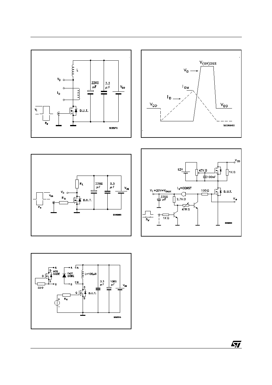
Fig. 1: Unclamped Inductive Load Test Circuit
Fig. 1: Unclamped Inductive Load Test Circuit
Fig. 2: Unclamped Inductive Waveform
Fig. 3: Switching Times Test Circuits For Resistive
Load
Fig. 4: Gate Charge test Circuit
Fig. 5: Test Circuit For Inductive Load Switching
And Diode Recovery Times
5/7
STB160NF3LL
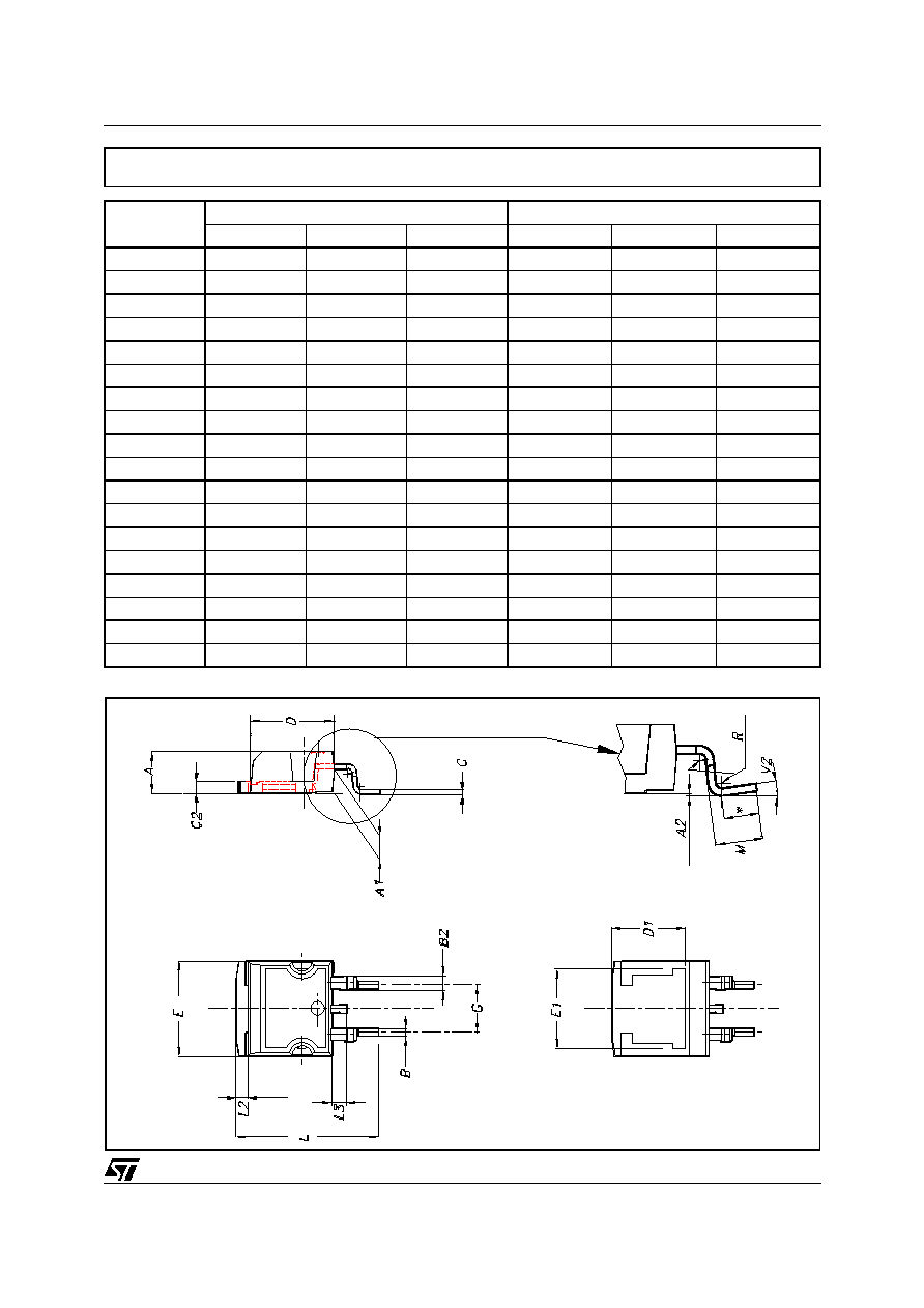
DIM.
mm.
inch.
MIN.
TYP. MAX.
MIN.
TYP. TYP.
A
4.4
4.6
0.173
0.181
A1
2.49
2.69
0.098
0.106
A2
0.03
0.23
0.001
0.009
B
0.7
0.93
0.028
0.037
B2
1.14
1.7
0.045
0.067
C
0.45
0.6
0.018
0.024
C2
1.21
1.36
0.048
0.054
D
8.95
9.35
0.352
0.368
D1
8
0.315
E
10
10.4
0.394
0.409
E1
8.5
0.334
G
4.88
5.28
0.192
0.208
L
15
15.85
0.591
0.624
L2
1.27
1.4
0.050
0.055
L3
1.4
1.75
0.055
0.069
M
2.4
3.2
0.094
0.126
R
0.4
0.015
V2
0∞
8∞
0∞
8∞
D
2
PAK MECHANICAL DATA