 | –≠–ª–µ–∫—Ç—Ä–æ–Ω–Ω—ã–π –∫–æ–º–ø–æ–Ω–µ–Ω—Ç: STB22NM50 | –°–∫–∞—á–∞—Ç—å:  PDF PDF  ZIP ZIP |
1/10
ADVANCED DATA
January 2003
STP22NM50 - STP22NM50FP
STB22NM50 - STB22NM50-1
N-CHANNEL 500V - 0.16
- 20A TO-220/FP/D
2
PAK/I
2
PAK
MDmeshTMPower MOSFET
s
TYPICAL R
DS
(on) = 0.16
s
HIGH dv/dt AND AVALANCHE CAPABILITIES
s
100% AVALANCHE TESTED
s
LOW INPUT CAPACITANCE AND GATE CHARGE
s
LOW GATE INPUT RESISTANCE
DESCRIPTION
The MDmeshTM is a new revolutionary MOSFET tech-
nology that associates the Multiple Drain process with
the Company's PowerMESHTM horizontal layout. The
resulting product has an outstanding low on-resis-
tance, impressively high dv/dt and excellent avalanche
characteristics. The adoption of the Company's propri-
etary strip technique yields overall dynamic perfor-
mance that is significantly better than that of similar
competition's products.
APPLICATIONS
The MDmeshTM family is very suitable for increasing
power density of high voltage converters allowing sys-
tem miniaturization and higher efficiencies.
ABSOLUTE MAXIMUM RATINGS
(∑)Pulse width limited by safe operating area
TYPE
V
DSS
R
DS(on)
R
ds(on)
*Q
g
I
D
STP22NM50
STP22NM50FP
STB22NM50
STB22NM50-1
500 V
500 V
500 V
500 V
<0.215
<0.215
<0.215
<0.215
6.4
*nC
6.4
*nC
6.4
*nC
6.4
*nC
20 A
20 A
20 A
20 A
Symbol
Parameter
Value
Unit
STP(B)22NM50(-1)
STP22NM50FP
V
DS
Drain-source Voltage (V
GS
= 0)
500
V
V
DGR
Drain-gate Voltage (R
GS
= 20 k
)
500
V
V
GS
Gate- source Voltage
±30
V
I
D
Drain Current (continuous) at T
C
= 25∞C
20
20(*)
A
I
D
Drain Current (continuous) at T
C
= 100∞C
12.6
12.6(*)
A
I
DM
(
q
)
Drain Current (pulsed)
80
80(*)
A
P
TOT
Total Dissipation at T
C
= 25∞C
192
45
W
Derating Factor
1.2
0.36
W/∞C
dv/dt(1)
Peak Diode Recovery voltage slope
15
V/ns
V
ISO
Insulation Winthstand Voltage (DC)
--
2000
V
T
stg
Storage Temperature
≠65 to 150
∞C
T
j
Max. Operating Junction Temperature
150
∞C
(1)I
SD
20A, di/dt
400A/µs, V
DD
V
(BR)DSS
, T
j
T
JMAX.
(*)Limited only by maximum temperature allowed
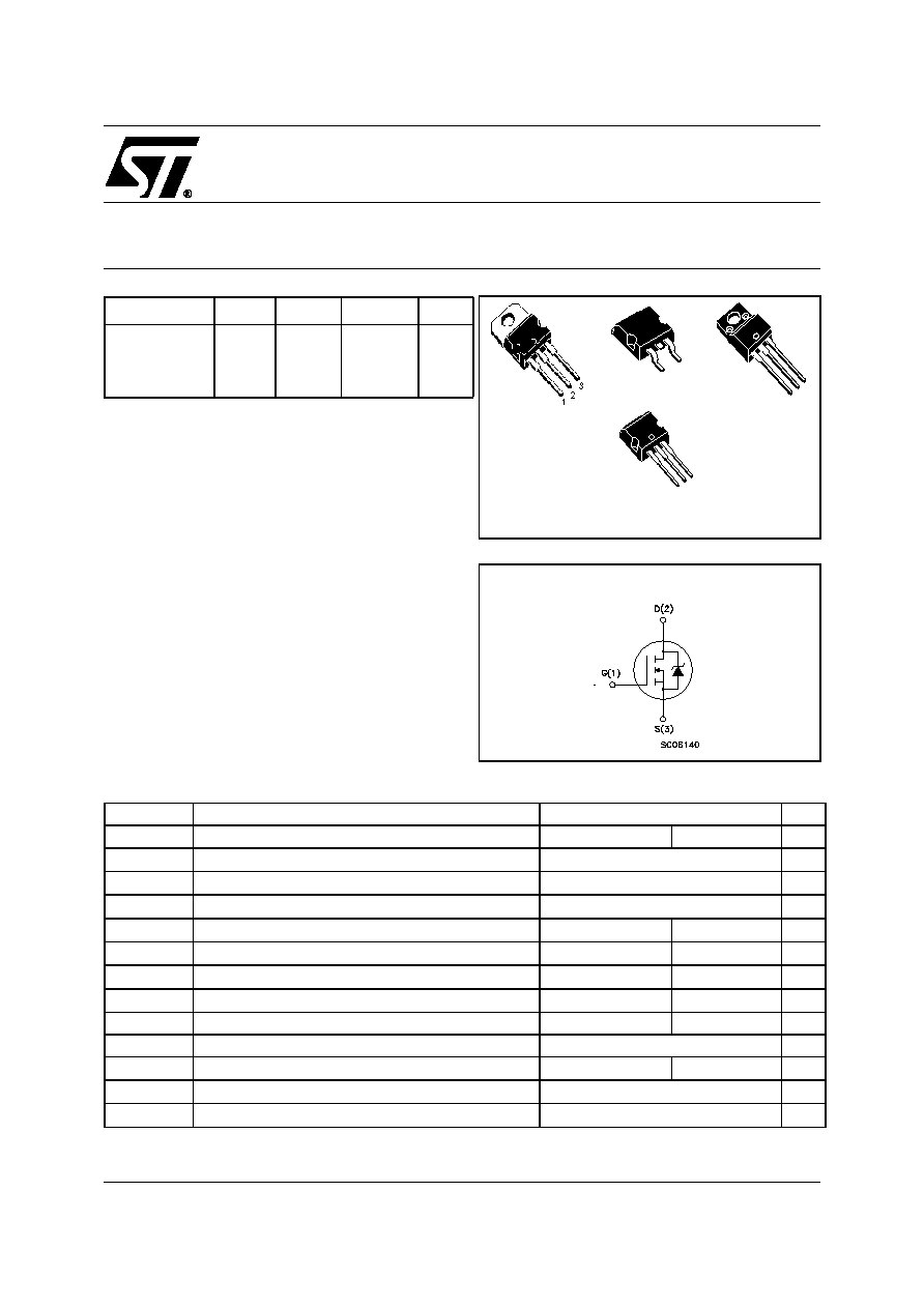
TO-220
1
2
3
TO-220FP
1
2
3
I≤PAK
(Tabless TO-220)
1
3
D
2
PAK
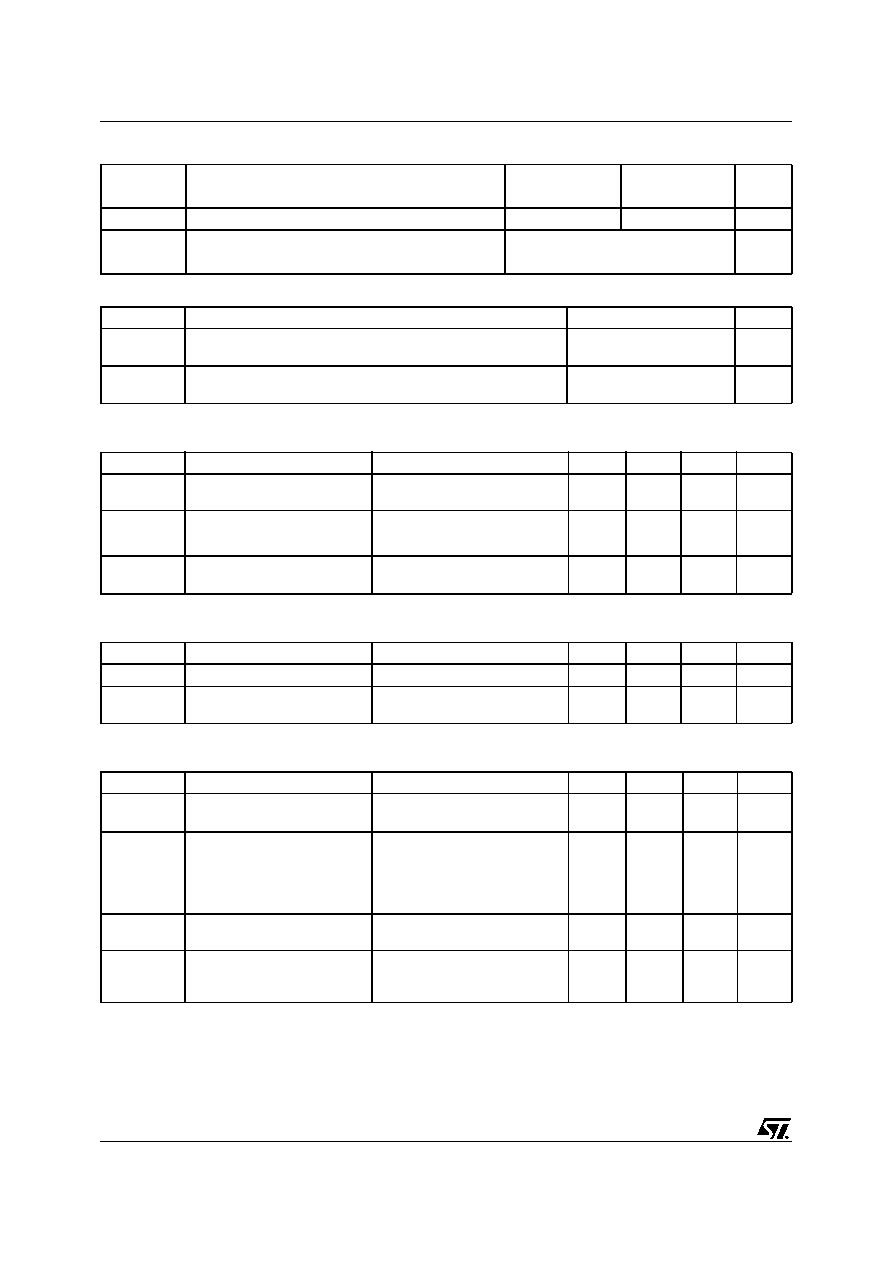
INTERNAL SCHEMATIC DIAGRAM
STP22NM50 / STP22NM50FP / STB22NM50 / STB22NM50-1
2/10
THERMAL DATA
AVALANCHE CHARACTERISTICS
ELECTRICAL CHARACTERISTICS (T
CASE
= 25 ∞C UNLESS OTHERWISE SPECIFIED)
OFF
ON (1)
DYNAMIC
1. Pulsed: Pulse duration = 300 µs, duty cycle 1.5 %.
2. C
oss eq.
is defined as a constant equivalent capacitance giving the same charging time as C
oss
when V
DS
increases from 0 to 80%
V
DSS
.
TO-220/I
2
PAK/
D
2
PAK
TO-220FP
Rthj-case
Thermal Resistance Junction-case
Max
0.65
2.8
∞C/W
Rthj-amb
Thermal Resistance Junction-ambient
Max
62.5
∞C/W
T
l
Maximum Lead Temperature For Soldering Purpose
300
∞C
Symbol
Parameter
Max Value
Unit
I
AR
Avalanche Current, Repetitive or Not-Repetitive
(pulse width limited by T
j
max)
10
A
E
AS
Single Pulse Avalanche Energy
(starting T
j
= 25 ∞C, I
D
= 5 A, V
DD
= 50 V)
650
mJ
Symbol
Parameter
Test Conditions
Min.
Typ.
Max.
Unit
V
(BR)DSS
Drain-source
Breakdown Voltage
I
D
= 250 µA, V
GS
= 0
500
V
I
DSS
Zero Gate Voltage
Drain Current (V
GS
= 0)
V
DS
= Max Rating
1
µA
V
DS
= Max Rating, T
C
= 125 ∞C
10
µA
I
GSS
Gate-body Leakage
Current (V
DS
= 0)
V
GS
= ±30V
±100
nA
Symbol
Parameter
Test Conditions
Min.
Typ.
Max.
Unit
V
GS(th)
Gate Threshold Voltage
V
DS
= V
GS
, I
D
= 250µA
3
4
5
V
R
DS(on)
Static Drain-source On
Resistance
V
GS
= 10V, I
D
= 10A
0.16
0.215
Symbol
Parameter
Test Conditions
Min.
Typ.
Max.
Unit
g
fs
(1)
Forward Transconductance
V
DS
> I
D(on)
x R
DS(on)max,
I
D
= 10A
10
S
C
iss
Input Capacitance
V
DS
= 25V, f = 1 MHz, V
GS
= 0
1480
pF
C
oss
Output Capacitance
285
pF
C
rss
Reverse Transfer
Capacitance
34
pF
C
oss eq.
(2)
Equivalent Output
Capacitance
V
GS
= 0V, V
DS
= 0V to 400V
130
pF
R
g
Gate Input Resistance
f=1 MHz Gate DC Bias=0
Test Signal Level=20mV
Open Drain
1.6
3/10
STP22NM50 / STP22NM50FP / STB22NM50 / STB22NM50-1
ELECTRICAL CHARACTERISTICS (CONTINUED)
SWITCHING ON
SWITCHING OFF
SOURCE DRAIN DIODE
Note: 1. Pulsed: Pulse duration = 300 µs, duty cycle 1.5 %.
2. Pulse width limited by safe operating area.
Symbol
Parameter
Test Conditions
Min.
Typ.
Max.
Unit
t
d(on)
Turn-on Delay Time
V
DD
= 250 V, I
D
= 10 A
R
G
= 4.7
V
GS
= 10 V
(see test circuit, Figure 3)
24
ns
t
r
Rise Time
16
ns
Q
g
Total Gate Charge
V
DD
= 400 V, I
D
= 20 A,
V
GS
= 10 V
40
56
nC
Q
gs
Gate-Source Charge
13
nC
Q
gd
Gate-Drain Charge
19
nC
Symbol
Parameter
Test Conditions
Min.
Typ.
Max.
Unit
t
r(Voff)
Off-voltage Rise Time
V
DD
= 400 V, I
D
= 20 A,
R
G
= 4.7
,
V
GS
= 10 V
(see test circuit, Figure 5)
9
ns
t
f
Fall Time
8.5
ns
t
c
Cross-over Time
23
ns
Symbol
Parameter
Test Conditions
Min.
Typ.
Max.
Unit
I
SD
Source-drain Current
20
A
I
SDM
(2)
Source-drain Current (pulsed)
80
A
V
SD
(1)
Forward On Voltage
I
SD
= 20 A, V
GS
= 0
1.5
V
t
rr
Q
rr
I
RRM
Reverse Recovery Time
Reverse Recovery Charge
Reverse Recovery Current
I
SD
= 20 A, di/dt = 100A/µs,
V
DD
= 100 V, T
j
= 25∞C
(see test circuit, Figure 5)
350
4.6
26
ns
µC
A
t
rr
Q
rr
I
RRM
Reverse Recovery Time
Reverse Recovery Charge
Reverse Recovery Current
I
SD
= 20 A, di/dt = 100A/µs,
V
DD
= 100 V, T
j
= 150∞C
(see test circuit, Figure 5)
435
5.9
27
ns
µC
A
STP22NM50 / STP22NM50FP / STB22NM50 / STB22NM50-1
4/10
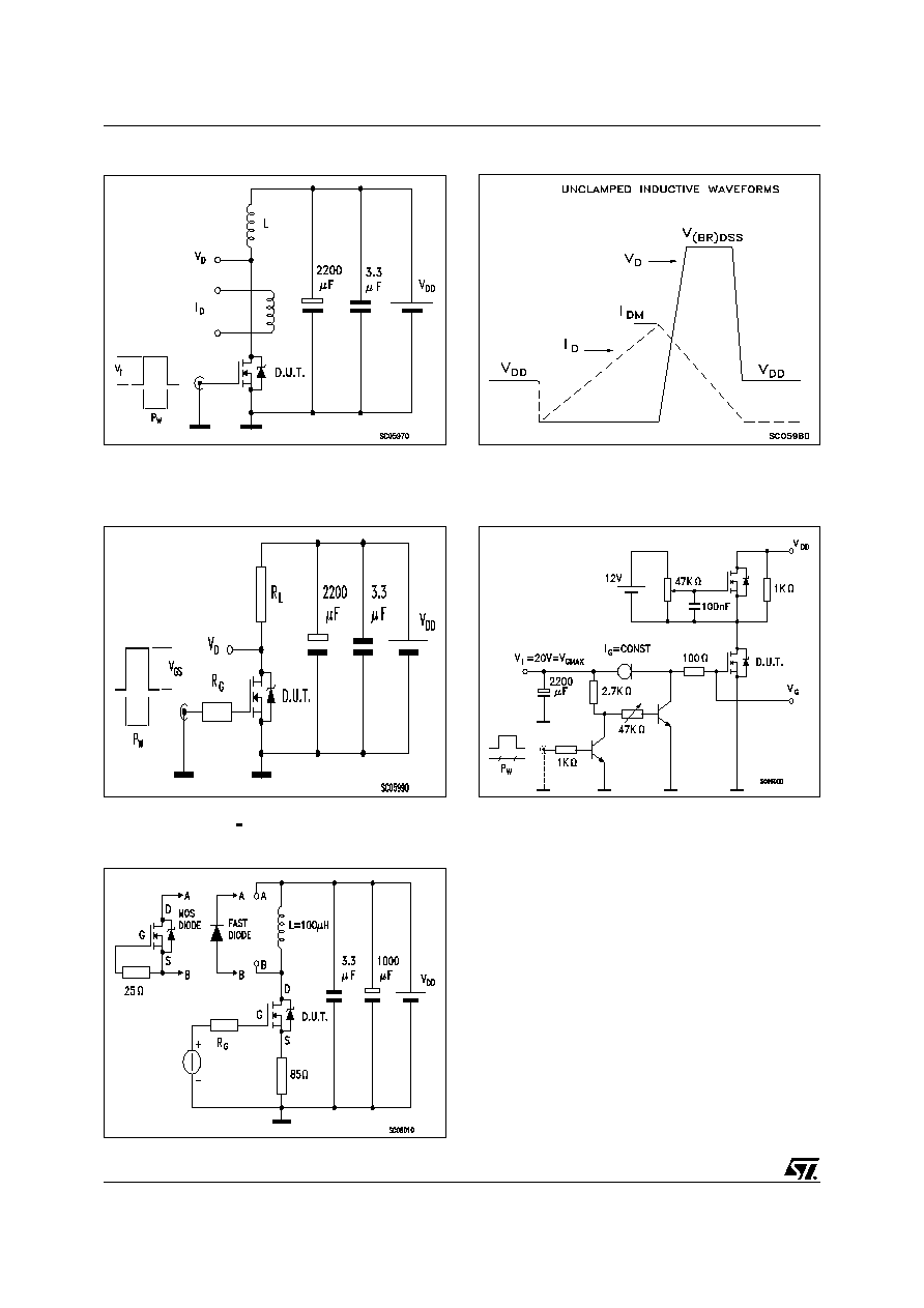
Fig. 5: Test Circuit For Inductive Load Switching
And Diode Recovery Times
Fig. 4: Gate Charge test Circuit
Fig. 2: Unclamped Inductive Waveform
Fig. 1: Unclamped Inductive Load Test Circuit
Fig. 3: Switching Times Test Circuits For
Resistive Load
5/10
STP22NM50 / STP22NM50FP / STB22NM50 / STB22NM50-1
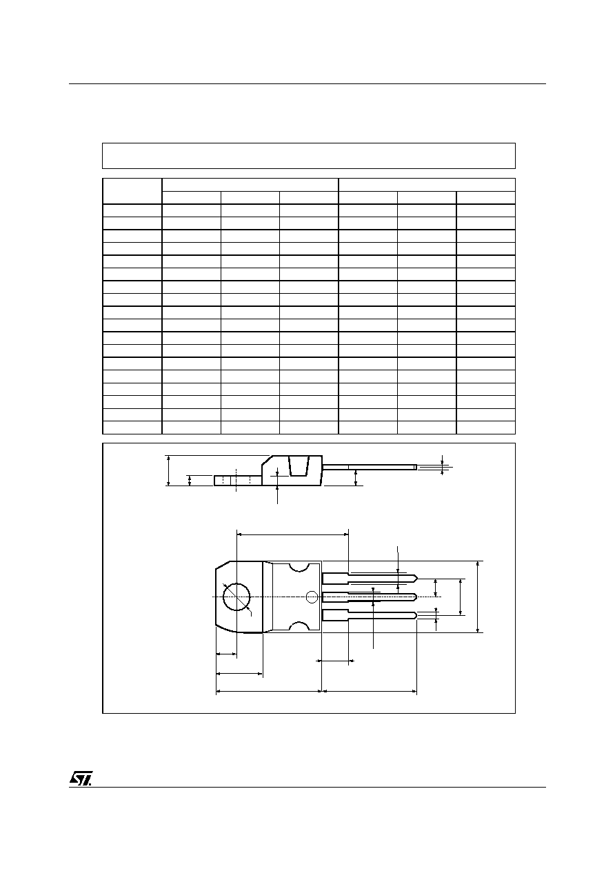
DIM.
mm
inch
MIN.
TYP.
MAX.
MIN.
TYP.
MAX.
A
4.40
4.60
0.173
0.181
C
1.23
1.32
0.048
0.051
D
2.40
2.72
0.094
0.107
D1
1.27
0.050
E
0.49
0.70
0.019
0.027
F
0.61
0.88
0.024
0.034
F1
1.14
1.70
0.044
0.067
F2
1.14
1.70
0.044
0.067
G
4.95
5.15
0.194
0.203
G1
2.4
2.7
0.094
0.106
H2
10.0
10.40
0.393
0.409
L2
16.4
0.645
L4
13.0
14.0
0.511
0.551
L5
2.65
2.95
0.104
0.116
L6
15.25
15.75
0.600
0.620
L7
6.2
6.6
0.244
0.260
L9
3.5
3.93
0.137
0.154
DIA.
3.75
3.85
0.147
0.151
L6
A
C
D
E
D1
F
G
L7
L2
Dia.
F1
L5
L4
H2
L9
F2
G1
TO-220 MECHANICAL DATA
P011C
STP22NM50 / STP22NM50FP / STB22NM50 / STB22NM50-1
6/10
1
DIM.
mm.
inch
MIN.
TYP
MAX.
MIN.
TYP.
MAX.
A
4.4
4.6
0.173
0.181
A1
2.49
2.69
0.098
0.106
A2
0.03
0.23
0.001
0.009
B
0.7
0.93
0.027
0.036
B2
1.14
1.7
0.044
0.067
C
0.45
0.6
0.017
0.023
C2
1.23
1.36
0.048
0.053
D
8.95
9.35
0.352
0.368
D1
8
0.315
E
10
10.4
0.393
E1
8.5
0.334
G
4.88
5.28
0.192
0.208
L
15
15.85
0.590
0.625
L2
1.27
1.4
0.050
0.055
L3
1.4
1.75
0.055
0.068
M
2.4
3.2
0.094
0.126
R
0.4
0.015
V2
0∫
8∫
D
2
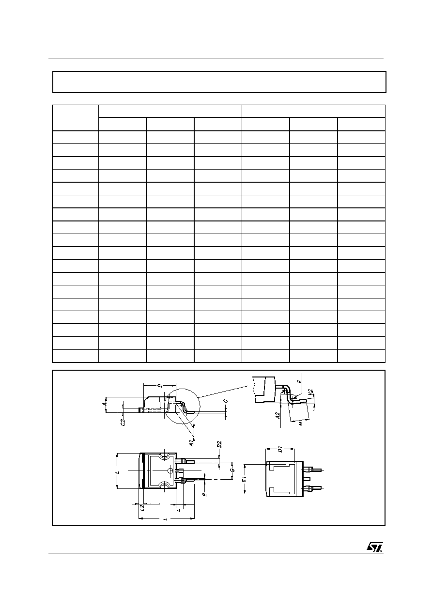
PAK MECHANICAL DATA
3
7/10
STP22NM50 / STP22NM50FP / STB22NM50 / STB22NM50-1
DIM.
mm
inch
MIN.
TYP.
MAX.
MIN.
TYP.
MAX.
A
4.4
4.6
0.173
0.181
B
2.5
2.7
0.098
0.106
D
2.5
2.75
0.098
0.108
E
0.45
0.7
0.017
0.027
F
0.75
1
0.030
0.039
F1
1.15
1.7
0.045
0.067
F2
1.15
1.7
0.045
0.067
G
4.95
5.2
0.195
0.204
G1
2.4
2.7
0.094
0.106
H
10
10.4
0.393
0.409
L2
16
0.630
L3
28.6
30.6
1.126
1.204
L4
9.8
10.6
0.385
0.417
L6
15.9
16.4
0.626
0.645
L7
9
9.3
0.354
0.366
ÿ
3
3.2
0.118
0.126
L2
A
B
D
E
H
G
L6
Ø
F
L3
G1
1 2 3
F2
F1
L7
L4
TO-220FP MECHANICAL DATA
STP22NM50 / STP22NM50FP / STB22NM50 / STB22NM50-1
8/10
DIM.
mm
inch
MIN.
TYP.
MAX.
MIN.
TYP.
MAX.
A
4.4
4.6
0.173
0.181
A1
2.49
2.69
0.098
0.106
B
0.7
0.93
0.027
0.036
B2
1.14
1.7
0.044
0.067
C
0.45
0.6
0.017
0.023
C2
1.23
1.36
0.048
0.053
D
8.95
9.35
0.352
0.368
e
2.4
2.7
0.094
0.106
E
10
10.4
0.393
0.409
L
13.1
13.6
0.515
0.531
L1
3.48
3.78
0.137
0.149
L2
1.27
1.4
0.050
0.055
L
L1
B2
B
D
E
A
C2
C
A1
L2
e
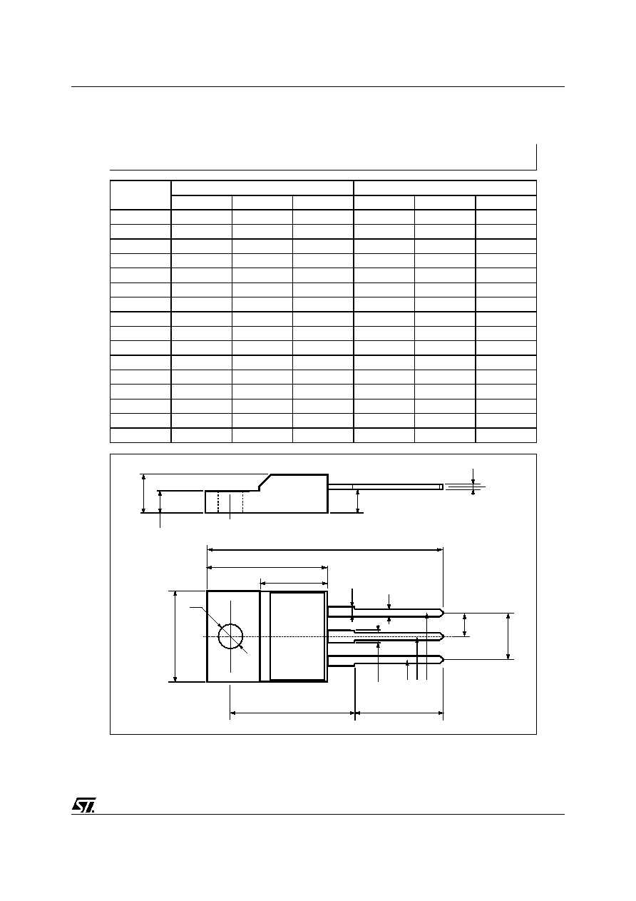
P011P5/E
TO-262 (I
2
PAK) MECHANICAL DATA
9/10
STP22NM50 / STP22NM50FP / STB22NM50 / STB22NM50-1
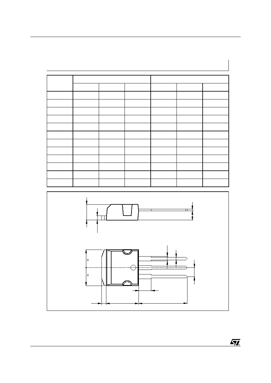
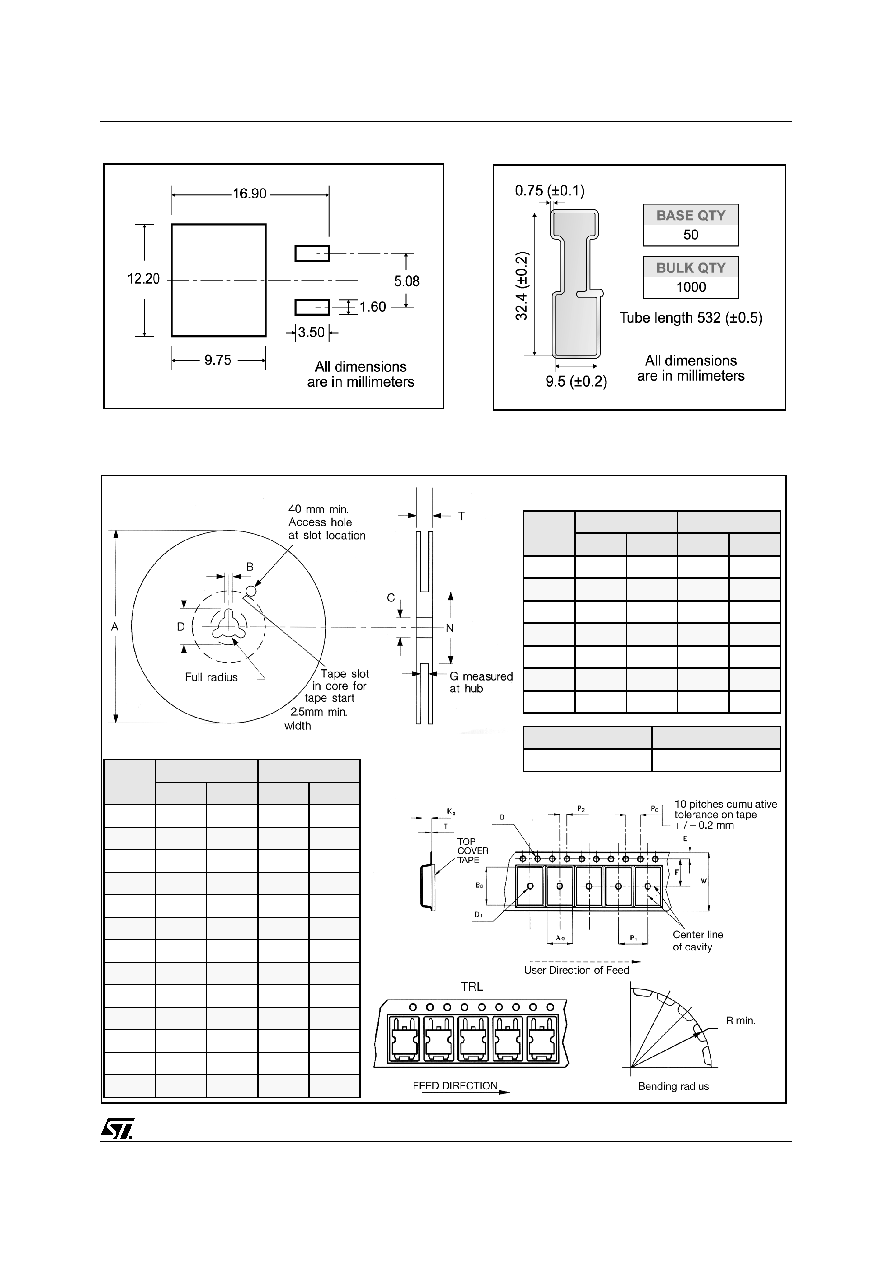
TAPE AND REEL SHIPMENT (suffix "T4")*
TUBE SHIPMENT (no suffix)*
D
2
PAK FOOTPRINT
* on sales type
DIM.
mm
inch
MIN.
MAX.
MIN.
MAX.
A
330
12.992
B
1.5
0.059
C
12.8
13.2
0.504
0.520
D
20.2
0795
G
24.4
26.4
0.960
1.039
N
100
3.937
T
30.4
1.197
BASE QTY
BULK QTY
1000
1000
REEL MECHANICAL DATA
DIM.
mm
inch
MIN.
MAX.
MIN.
MAX.
A0
10.5
10.7
0.413
0.421
B0
15.7
15.9
0.618
0.626
D
1.5
1.6
0.059
0.063
D1
1.59
1.61
0.062
0.063
E
1.65
1.85
0.065
0.073
F
11.4
11.6
0.449
0.456
K0
4.8
5.0
0.189
0.197
P0
3.9
4.1
0.153
0.161
P1
11.9
12.1
0.468
0.476
P2
1.9
2.1
0.075
0.082
R
50
1.574
T
0.25
0.35
0.0098 0.0137
W
23.7
24.3
0.933
0.956
TAPE MECHANICAL DATA

STP22NM50 / STP22NM50FP / STB22NM50 / STB22NM50-1
10/10
Information furnished is believed to be accurate and reliable. However, STMicroelectronics assumes no responsibility for the
consequences of use of such information nor for any infringement of patents or other rights of third parties which may result from
its use. No license is granted by implication or otherwise under any patent or patent rights of STMicroelectronics. Specifications
mentioned in this publication are subject to change without notice. This publication supersedes and replaces all information
previously supplied. STMicroelectronics products are not authorized for use as critical components in life support devices or
systems without express written approval of STMicroelectronics.
© The ST logo is a registered trademark of STMicroelectronics
© 2002 STMicroelectronics - Printed in Italy - All Rights Reserved
STMicroelectronics GROUP OF COMPANIES
Australia - Brazil - Canada - China - Finland - France - Germany - Hong Kong - India - Israel - Italy - Japan - Malaysia - Malta - Morocco
Singapore - Spain - Sweden - Switzerland - United Kingdom - United States.
© http://www.st.com