 | –≠–ª–µ–∫—Ç—Ä–æ–Ω–Ω—ã–π –∫–æ–º–ø–æ–Ω–µ–Ω—Ç: STB45NF06 | –°–∫–∞—á–∞—Ç—å:  PDF PDF  ZIP ZIP |
1/6
PRELIMINARY DATA
Aug 2000
This is preliminary information on a new product now in development or undergoing evaluation. Details are subject to change without notice.
STB45NF06
N-CHANNEL 60V - 0.022
- 38A D2PAK
STripFETTM POWER MOSFET
(1) I
SD
38A, di/dt
300A/µs, V
DD
V
(BR)DSS
, T
j
T
JMAX.
s
TYPICAL R
DS
(on) = 0.022
s
EXCEPTIONAL dv/dt CAPABILITY
DESCRIPTION
This Power Mosfet is the latest development of
STMicroelectronics unique "Single Feature
Size
TM"
strip-based process. The resulting tran-
sistor shows extremely high packing density for
low on-resistance, rugged avalance characteris-
tics and less critical alignment steps therefore a re-
markable manufacturing reproducibility.
APPLICATIONS
s
HIGH-EFFICIENCY DC-DC CONVERTERS
s
SOLENOID AND RELAY DRIVERS
s
MOTOR CONTROL, AUDIO AMPLIFIERS
s
DC-DC & DC-AC CONVERTERS
ABSOLUTE MAXIMUM RATINGS
(
q
) Pulse width limited by safe operating area
TYPE
V
DSS
R
DS(on)
I
D
STB45NF06
60V
<0.028
38A
Symbol
Parameter
Value
Unit
V
DS
Drain-source Voltage (V
GS
= 0)
60
V
V
DGR
Drain-gate Voltage (R
GS
= 20 k
)
60
V
V
GS
Gate- source Voltage
±20
V
I
D
Drain Current (continuos) at T
C
= 25∞C
38
A
I
D
Drain Current (continuos) at T
C
= 100∞C
26
A
I
DM
(
q
)
Drain Current (pulsed)
152
A
P
TOT
Total Dissipation at T
C
= 25∞C
80
W
Derating Factor
0.53
W/∞C
dv/dt (1)
Peak Diode Recovery voltage slope
7
V/ns
T
stg
Storage Temperature
≠65 to 175
∞C
T
j
Max. Operating Junction Temperature
175
∞C
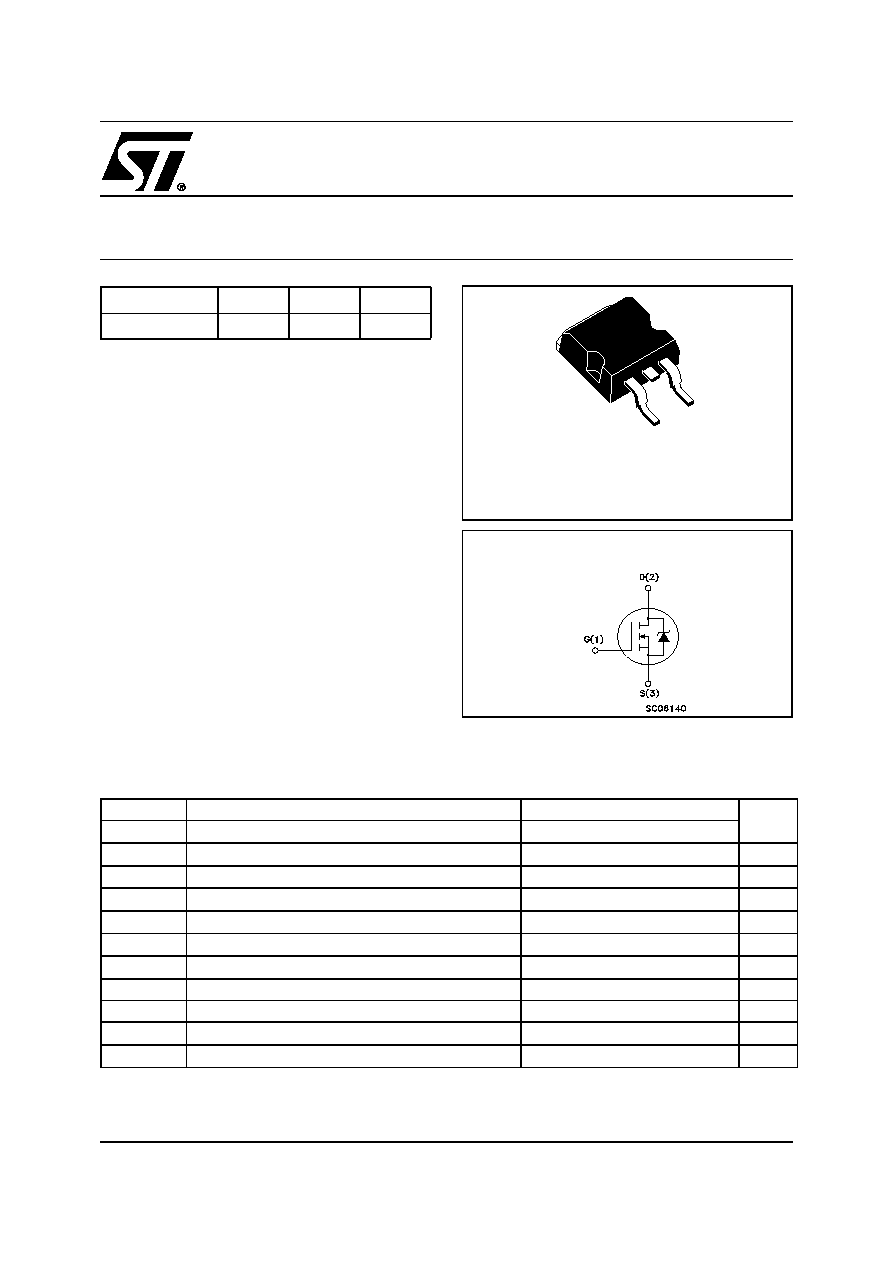
D2PAK
1
3
INTERNAL SCHEMATIC DIAGRAM
STB45NF06
2/6
THERMAL DATA
AVALANCHE CHARACTERISTICS
ELECTRICAL CHARACTERISTICS (TCASE = 25 ∞C UNLESS OTHERWISE SPECIFIED)
OFF
ON
(1)
DYNAMIC
Rthj-case
Thermal Resistance Junction-case Max
1.87
∞C/W
Rthj-amb
Thermal Resistance Junction-ambient Max
62.5
∞C/W
T
l
Maximum Lead Temperature For Soldering Purpose
300
∞C
Symbol
Parameter
Max Value
Unit
I
AR
Avalanche Current, Repetitive or Not-Repetitive
(pulse width limited by T
j
max)
38
A
E
AS
Single Pulse Avalanche Energy
(starting T
j
= 25 ∞C, I
D
= I
AR
, V
DD
= 50 V)
135
mJ
Symbol
Parameter
Test Conditions
Min.
Typ.
Max.
Unit
V
(BR)DSS
Drain-source
Breakdown Voltage
I
D
= 250 µA, V
GS
= 0
60
V
I
DSS
Zero Gate Voltage
Drain Current (V
GS
= 0)
V
DS
= Max Rating
1
µA
V
DS
= Max Rating, T
C
= 125 ∞C
10
µA
I
GSS
Gate-body Leakage
Current (V
DS
= 0)
V
GS
= ±20V
±100
nA
Symbol
Parameter
Test Conditions
Min.
Typ.
Max.
Unit
V
GS(th)
Gate Threshold Voltage
V
DS
= V
GS
, I
D
= 250µA
2
3
4
V
R
DS(on)
Static Drain-source On
Resistance
V
GS
= 10 V, I
D
= 19 A
0.022
0.028
I
D(on)
On State Drain Current
V
DS
> I
D(on)
x R
DS(on)max,
V
GS
= 10V
45
A
Symbol
Parameter
Test Conditions
Min.
Typ.
Max.
Unit
g
fs
(1)
Forward Transconductance
V
DS
> I
D(on)
x R
DS(on)max,
I
D
=19 A
24
S
C
iss
Input Capacitance
V
DS
= 25V, f = 1 MHz, V
GS
= 0
1730
pF
C
oss
Output Capacitance
215
pF
C
rss
Reverse Transfer
Capacitance
63
pF

3/6
STB45NF06
ELECTRICAL CHARACTERISTICS (CONTINUED)
SWITCHING ON
SWITCHING OFF
SOURCE DRAIN DIODE
Note: 1. Pulsed: Pulse duration = 300 µs, duty cycle 1.5 %.
2. Pulse width limited by safe operating area.
Symbol
Parameter
Test Conditions
Min.
Typ.
Max.
Unit
t
d(on)
Turn-on Delay Time
V
DD
= 30V, I
D
= 19A
R
G
= 4.7
V
GS
= 10V
(see test circuit, Figure 3)
20
ns
t
r
Rise Time
100
ns
Q
g
Total Gate Charge
V
DD
= 48V, I
D
= 38A,
V
GS
= 10V
43
58
nC
Q
gs
Gate-Source Charge
9
nC
Q
gd
Gate-Drain Charge
15
nC
Symbol
Parameter
Test Conditions
Min.
Typ.
Max.
Unit
t
d(off)
Turn-off-Delay Time
V
DD
= 30V, I
D
= 19A,
R
G
= 4.7
,
V
GS
= 10V
(see test circuit, Figure 3)
50
ns
t
f
Fall Time
20
ns
t
d(off)
Off-voltage Rise Time
Vclamp =48V, I
D
=38A
R
G
= 4.7
,
V
GS
= 10V
45
ns
t
f
Fall Time
(see test circuit, Figure 5)
42
ns
t
c
Cross-over Time
60
ns
Symbol
Parameter
Test Conditions
Min.
Typ.
Max.
Unit
I
SD
Source-drain Current
38
A
I
SDM
(1)
Source-drain Current (pulsed)
152
A
V
SD
(2)
Forward On Voltage
I
SD
= 38A, V
GS
= 0
1.5
V
t
rr
Reverse Recovery Time
I
SD
= 38A, di/dt = 100A/µs,
V
DD
= 100V, T
j
= 150∞C
(see test circuit, Figure 5)
95
ns
Q
rr
Reverse Recovery Charge
260
nC
I
RRM
Reverse Recovery Current
5.5
A
STB45NF06
4/6
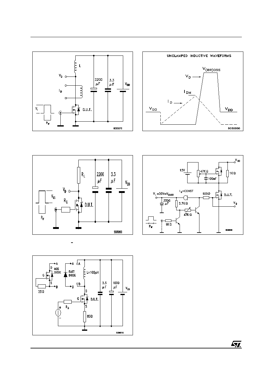
Fig. 5: Test Circuit For Inductive Load Switching
And Diode Recovery Times
Fig. 4: Gate Charge test Circuit
Fig. 2: Unclamped Inductive Waveform
Fig. 1: Unclamped Inductive Load Test Circuit
Fig. 3: Switching Times Test Circuit For
Resistive Load
5/6
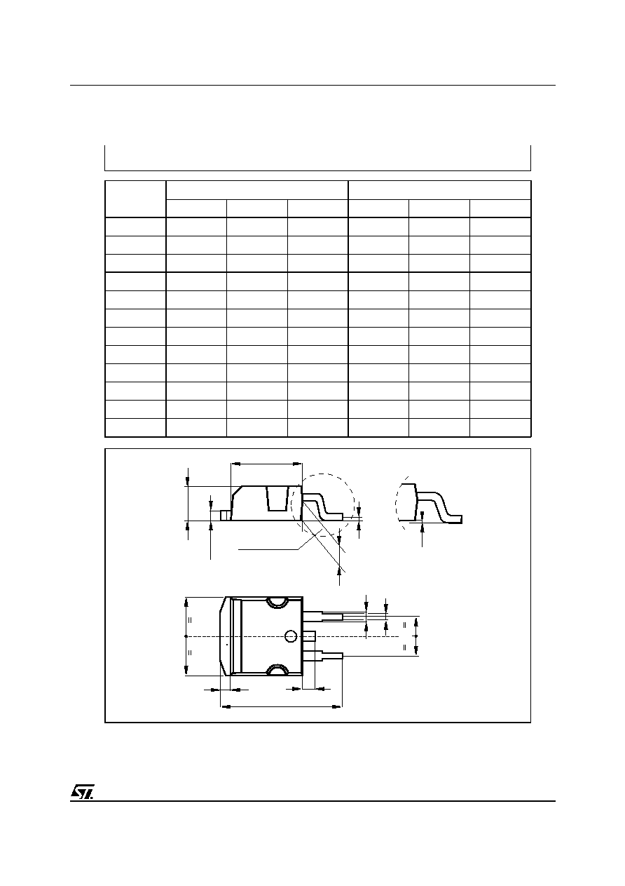
STB45NF06
DIM.
mm
inch
MIN.
TYP.
MAX.
MIN.
TYP.
MAX.
A
4.4
4.6
0.173
0.181
A1
2.49
2.69
0.098
0.106
B
0.7
0.93
0.027
0.036
B2
1.14
1.7
0.044
0.067
C
0.45
0.6
0.017
0.023
C2
1.21
1.36
0.047
0.053
D
8.95
9.35
0.352
0.368
E
10
10.4
0.393
0.409
G
4.88
5.28
0.192
0.208
L
15
15.85
0.590
0.624
L2
1.27
1.4
0.050
0.055
L3
1.4
1.75
0.055
0.068
L2
L3
L
B2
B
G
E
A
C2
D
C
A1
DET AIL "A"
DET AIL "A"
A2
P011P6/E
TO-263 (D
2
PAK) MECHANICAL DATA