 | –≠–ª–µ–∫—Ç—Ä–æ–Ω–Ω—ã–π –∫–æ–º–ø–æ–Ω–µ–Ω—Ç: STB5600 | –°–∫–∞—á–∞—Ç—å:  PDF PDF  ZIP ZIP |
STB5600
GPS RF FRONT-END IC
s
ONE CHIP SYSTEM TO INTERFACE
ACTIVE ANTENNA TO ST20GP1
MICROCONTROLLER
s
COMPLETE RECEIVER USING NOVEL
DUAL CONVERSION ARCHITECTURE WITH
SINGLE IF FILTER
s
MINIMUM EXTERNAL COMPONENTS
s
COMPATIBLE WITH GPS L1 SPS SIGNAL
s
INTERNALLY STABILISED POWER RAILS
s
CMOS OUTPUT LEVELS
s
FROM 3.3 TO 5.9V SUPPLY VOLTAGE
s
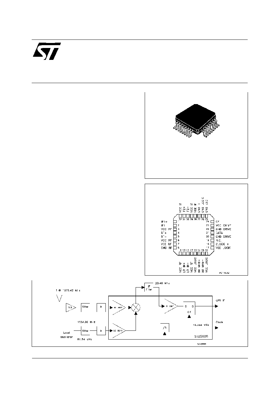
TQFP32 PACKAGE
DESCRIPTION
The STB5600, using STMicroelectronics HSB2,
High Speed Bipolar technology, implements a
Global Positioning System RF front-end.
The chip provides down conversion from the GPS
(L1) signal at 1575 MHz via an IF of 20MHz to an
output frequency of 4MHz suitable for ST20GP1
GPS processor.
It uses a single external reference oscillator to
generate both RF local oscillator signals and the
processor reference clock.
Æ
PIN CONNECTION (top view)
August 1998
TQFP32
MARKING:
STB5600
TRACEAB. CODE
ASSY CODE
1/10

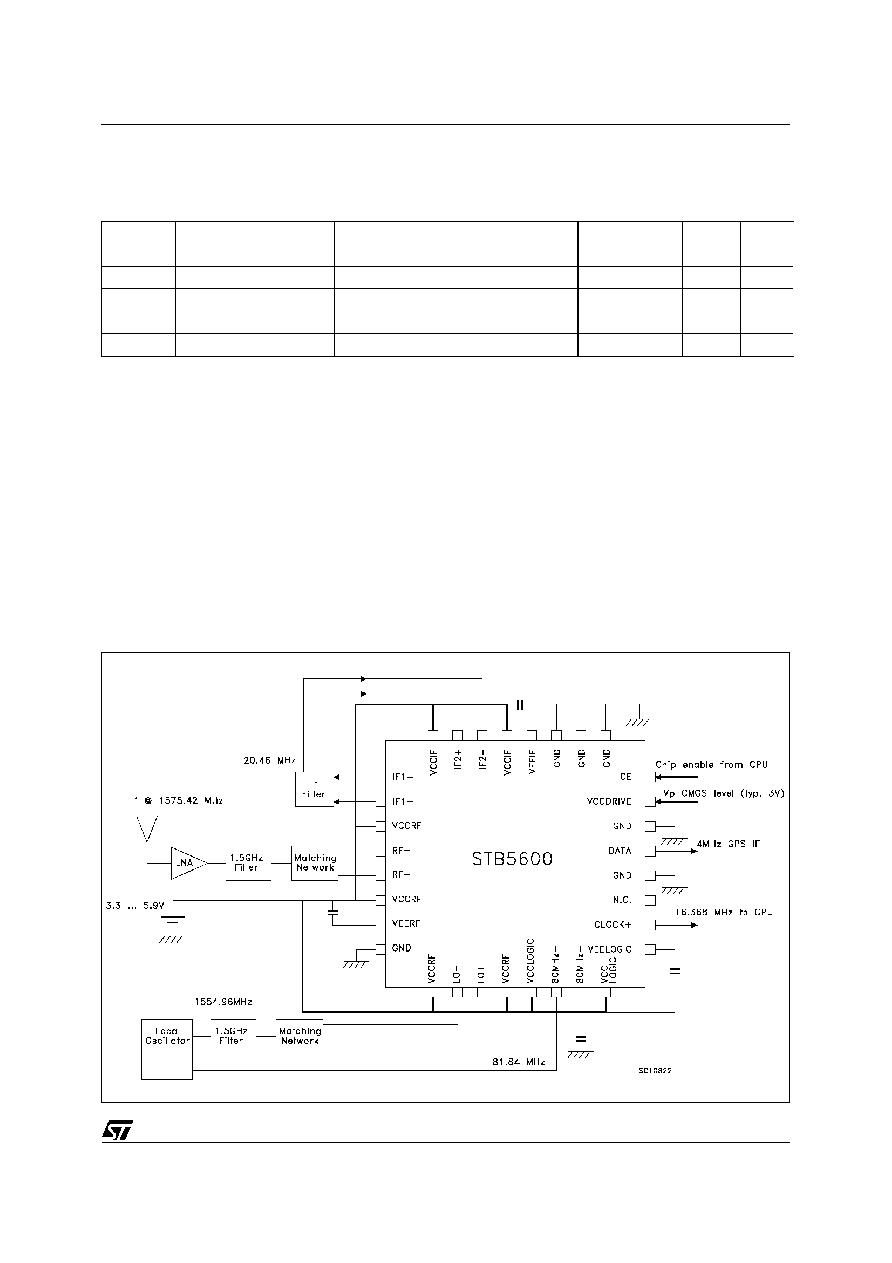
FUNCTIONAL DESCRIPTION
The STB5600 GPS front-end is fed with the signal from an active antenna, via a ceramic RF filter. The
gain between the antenna element
and the STB5600 is expected to be between 10dB and 35dB
overall, made up of the antenna LNA gain, the feeder loss, connector loss, and the ceramic filter loss.
In order to use an off-the-shelf ceramic filter, conventionally 50 Ohms single ended, a matching circuit is
used. (see appendix A.1), which provides a 300 Ohm differential drive to the STB5600. A similar circuit
can be used to feed the LO signal if using the recommended low-cost oscillator circuit (appendix A.3).
Note that the STB5600 radio architecture and the oscillator described here are covered by various
patents held by SGS-Thomson and by others. The use of the circuits described in this data-sheet for any
other purpose may infringe such patents.
-
RF SECTION
The differential input signal is amplified by the RF-Amp and mixed with the oscillator signal amplified
from the LO+,LO- inputs to generate a balanced 20.46MHz IF signal. The LO buffer amplifier may be
fed differential or single ended signals, at levels between -60dBm and -20dBm .
-
IF SECTION
The 20MHz differential signal from the mixer is fed through an external LC filter to suppress undesirable
signals and mixer products. The multi-stage high-sensitivity limiting amplifier is connected to a D-type
latch clocked by an internally derived 16MHz clock.. The effect of sampling the 20MHz signal at 16MHz
is to create a sub-sampling alias at 4MHz. This is fed to the output level-converters.
-
DIVIDER SECTION
The 80MHz oscillator signal may be provided single-ended or differentially to the high impedance
80MHz+, 80MHz- inputs. Any unused inputs should be connected to GNDLOGIC via a 1nF capacitor.
The 80MHz signal is amplified, then divided by 5 to create the 16.368MHz clock required by the
ST20GP1 processor, also used to clock the output latch of the STB5600.
-
OUTPUT SECTION
The output latch samples the 20.46MHz intermediate frequency at a 16.368MHz rate, performing the
dual function of second downconversion and latching. The downconversion occurs by sub-sampling
aliasing, such that the digital output represents a 4.096MHz centre frequency
The output buffers perform level translation from the internal ECL levels to CMOS compatible outputs
referred to external ground.
ABSOLUTE MAXIMUM RATINGS
Symbol
Parameter
Val ue
Uni t
V
CC
DC Supply Voltage
5.9
V
RF+, RF- RF I nput
8
dBm
T
j
Junct ion Temperature
150
o
C
T
stg
St orage Temperature Range
-40 to 125
o
C
R
thj-a mb
Thermal Resistance Junction-ambient
80
o
C/W
STB5600
2/10
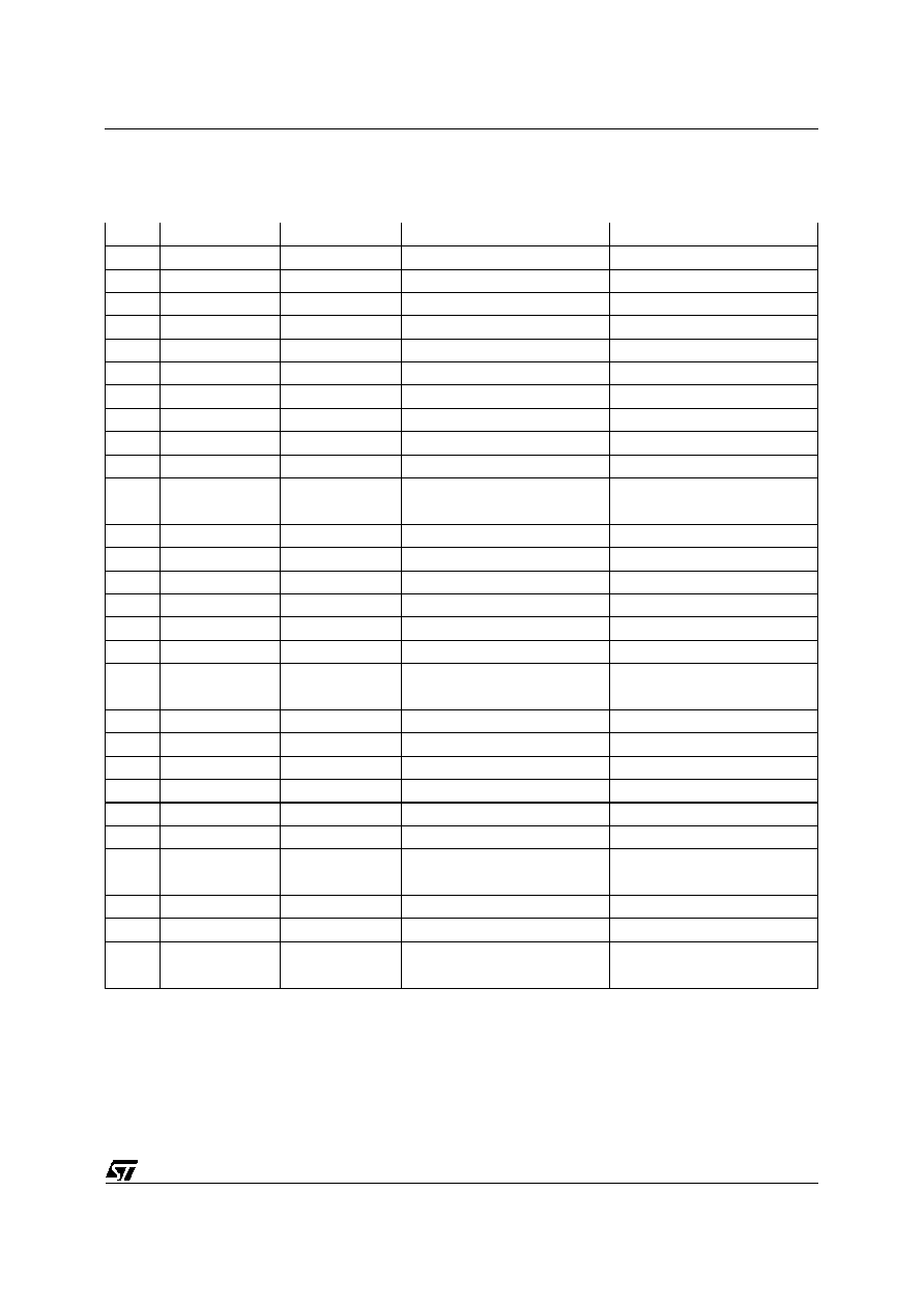
PIN CONFIGURATION
Apply 5V at the CE, V
CCRF
, V
CCIF
, V
CCLOGIC
pins, apply 3 V at the V
CCDRIV E
Pin
Symbol
Typ. DC Bias
Dexription
Extern al circuit
1
I F1+
3.6 V
Mixer O utput 1
see application circuit
2
IF 1-
3.6 V
Mixer O utput 2
see application circuit
3
V
CCRF
5 V
RF Power Supply
100 nF t o V
EERF
4
RF+
3.5 V
RF Input
AC Coupled
5
RF -
3.5 V
RF Input
AC Coupled
6
V
CCRF
5 V
RF Power Supply
100 nF to VEERF
7
V
EERF
2 V
RF Voltage Reference
100 nF to VCCRF
8
GNDRF
0 V
RF Ground
9
V
CCRF
5 V
RF Power Supply
100 nF to VEERF
10
LO+
3.5 V
Local Oscillator Input
AC Coupled
11
LO -
3.5 V
Local Oscillator Input
AC Coupled
12
V
CCRF
5 V
RF Power Supply
100 nF to VEERF
13
V
CCLOGI C
5 V
Logic Power Supply
100 nF to VEELOGI C
14
80 MHz+
4 V
80 MHz Clock Input
AC Coupled
15
80 MHz-
4 V
80 MHz Clock Input
AC Coupled
16
V
CCLOGI C
5 V
Logic Power Supply
100 nF to VEELOGI C
17
V
EELO GIC
2 V
Logic Volt age Reference
100 nF to VCCLOG IC
18
CLOCK+
0.3 V or 3 V
16 MHz Clock CMOS Output
7 pF to G ND
DRIVE
19
Not Connected
20
GND
DRIVE
0 V
CMO S Drive Ground
21
DATA
0.3 V or 3 V
4 MHz Dat a CMOS Output
7 pF to G ND
DRIVE
22
GND
DRIVE
0 V
CMO S Drive Ground
23
V
CCDRIVE
3 V
CMO S Drive Power Supply
24
CE
3 V
Chip Enable
25
G ND
0 V
Substrate Ground
26
GND
LO GIC
0 V
Logic G round
27
GND
IF
0 V
IF Ground
28
V
EEIF
2 V
IF Volt age Ref erence
100 nF to VCCIF
29
V
CCI F
5 V
IF Power Supply
100 nF t o VEEIF
30
IF 2-
4 V
Limit ing Amplif ier Input
see application circuit
31
I F2+
4 V
Limit ing Amplif ier Input
see application circuit
32
V
CCI F
5 V
IF Power Supply
100 nF t o VEEIF
STB5600
3/10
ELECTRICAL SPECIFICATION (V
VCCRF
= 3.3 V ...5.9 V; V
VCCIF
= 3.3 V ...5.9 V; V
VCC LOGIC
= 3.3 V
...5.9 V V
VCCDRIVE
= 3 V; T
a
= 25
o
C unless otherwise specified)
LNA MIXER
Symb ol
Parameter
Note
Mi n.
Typ .
Max.
Un it
I
VCCRF
Supply Current
VVCCRF = 5 V
20
25
mA
Z
in
Differential Input
Impedance
@ 1575 MHz AC Coupled at RF+
RF - inputs
300
1
pF
Z
out
Differential Out put
Impedance
@ 20 MHz AC Coupled at IF1+ IF1-
out puts
70
3
pF
G
C
Voltage Conversion
Gain
R
L
> 3K
,
P
I N
= -80 dBm
(V
in
= 75
µ
Vp on 300
)
35
dB
IIP1
Input Compression
Point (1dB)
(see application circuit)
-60
dBm
NF
Noise figure
5
dB
f
RF
Input Signal
Frequency (L1)
1575
MHz
f
IF
Output Signal
Frequency
20
MHz
LO INPUT BUFFER
Symb ol
Parameter
Note
Mi n.
Typ .
Max.
Un it
Z
in
Differential Input
Impedance
@ 1555 MHz AC Coupled at LO+
LO - inputs
300
1
pF
Input Signal Level
-60
-40
-20
dBm
LIMITING AMPLIFIER
Symb ol
Parameter
Note
Mi n.
Typ .
Max.
Un it
I
VCCIF
Supply Current
VVCCI F = 5 V
2. 5
3.5
mA
Z
in
Differential Input
Impedance
@ 20 MHz AC Coupled at IF2+ IF2-
input s
15
K
B
Bandwidt h 3dB
5
80
MHz
Sens
Limiter sensit ivit y
Input Signal @ 20 MHz AC Coupled
100
µ
Vp
V
I NMAX
Maximum Input Signal
Input Signal @ 20 MHz AC Coupled
0.5
Vp
CLOCK INPUT BUFFER
Symb ol
Parameter
Note
Mi n.
Typ .
Max.
Un it
I
VCCLOGIC
Supply Current
VVCC LOGI C = 5 V
5
7
mA
Z
in
Differential Input
Impedance
@ 80 MHz AC Coupled at 8O MHz+
80 MHz- input s
8
2
K
pF
Input Signal Level
@ 80 MHz AC Coupled at 8O MHz+
80 MHz- input s
5
100
mVp
N
Division Ratio
5
STB5600
4/10
ELECTRICAL CHARACTERISTICS (Continued)
OUTPUT SECTION
Symb ol
Parameter
Note
Mi n.
Typ .
Max.
Unit
I
VCCDRI VE
Supply Current
V
VCCDRI VE
= 3 V
8
mA
V
O H
High output voltage
Vp = V
VCCDRIVE
= 3 V
Vp-0.4
Vp
V
V
OL
Low output volt age
Vn = GNDDRIVE
Vn
Vn+0. 4
V
t
r
Rise Time
C
LOAD
= 7 pF
6
ns
t
f
Fall T ime
C
LOAD
= 7 pF
2
ns
APPLICATION CIRCUIT
A typical application circuit is shown in figure 1. The RF input from the antenna downlead is fed via a
ceramic filter and matching circuit to the RF+,RF- pins. The external LNA in the antenna should have
between 10 and 35dB of amplifier gain, so the noise measured in a one MHz bandwidth should be
-114dBm for kTB in 1 MHz
+ 2dB LNA noise figure
+10/35 dB LNA gain (net)
Total -102/ 77dBm at connector.
Allowing 2dB for filter loss, -104/-79 is available at the matching circuit.
Fig. 1 Typical Application Circuit
STB5600
5/10