1/11
PRELIMINARY DATA
May, 7 2002
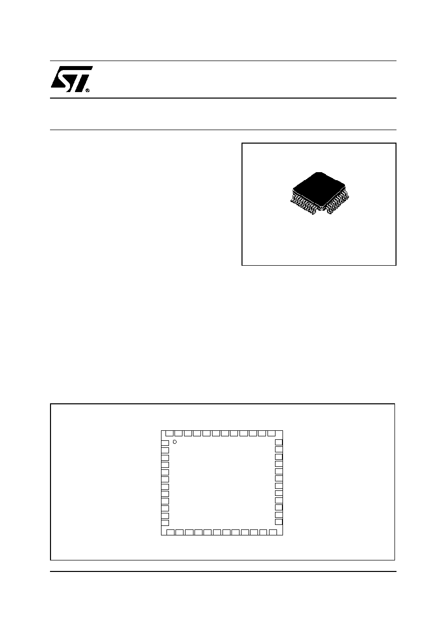
STB5610
GPS RF FRONT-END IC
TQFP48
ORDER CODE
STB5610
BRANDING
STB5610
∑ ONE CHIP SYSTEM TO INTERFACE GPS
ANTENNA TO GPS MICRO CONTROLLER
∑ ABLE TO SUPPORT ACTIVE AND PASSIVE
ANTENNA
∑ MINIMUM EXTERNAL COMPONENTS
∑ COMPATIBLE WITH GPS L1 SPS SIGNAL AND
GALILEO FREQUENCIES
∑ CMOS OUTPUT LEVELS
∑ 2.7 V .. 3.6 V SUPPLY VOLTAGE
∑ EMBEDDED LOW PHASE NOISE PLL
∑ ACTIVE ANTENNA SENSOR
∑ SMART CHIP ENABLE FUNCTION FOR POWER
CONSUMPTION OPTIMIZATION
∑ ESD PROTECTED
DESCRIPTION
The STB5610, using ST Microelectronics RF Bipolar
technology, implements a Global Positioning System
RF front-end. The chip provides down conversion
from the 1575.42 MHz GPS (L1) signal to 4.092 MHz
Output signal. The integrated PLL with on-chip
reference oscillator uses a low cost 16.368 MHz
crystal. No TCXO is required.
48
47
46
45
44
43
42
41
40
39
38
13
14
15
16
17
18
19
20
21
22
23
24
1
2
3
4
5
6
7
8
9
10
11
12
36
35
34
33
32
31
30
29
28
27
26
25
Vcc_XTAL
Vcc_Logic
LF
Vcc_VCO
Gnd
TNK1
TNK2
Gnd
Gnd
IF1+
IF1-
Gnd
1
2
3
4
5
6
7
8
9
10
11
48
47
46
45
44
43
42
41
40
39
38
48
47
46
45
44
43
42
41
40
39
38
37
48
47
46
45
44
43
42
41
40
39
38
CE
2
G
n
d
_
X
T
A
L
X
T
A
L_out
X
T
A
L
_
i
n
G
n
d
_
X
T
A
L
V
c
c
_
I
F
G
n
d
_
I
F
IF
2+
I
F
2
-
Gn
d
_
I
F
F
s
el
ec
t
C
E
Gn
d
_
R
F
G
n
d
LN
A
_
i
n
+
L
N
A
_
i
n
-
G
n
d
V
c
c
_
L
N
A
L
N
A
_
o
u
t
-
LN
A
_out+
V
c
c
_
R
F
G
nd_R
F
RF
-
R
F
+
Vcc_Logic2
Gnd
CLK
Gnd_Driver
Vcc_Driver
Gnd_Loic
Vcc_Logic
AS1
AS2
GC
As_out
DATA
PIN CONNECTION

STB5610
4/11
Data @ 4 MHz
CMOS levels
CLK @ 16MHz
CMOS levels
SAW Filter
16.368 MHz
Quartz
Two gain
LNA
D
CK
Q
PLL
~
1.55 GHz
20 MHz
Passive
Antenna
RF Amp.
Mixer
D Latch Output buffer
VCO
ExternalTank
1.57 GHz
Gain
Select.
CE
CE2
Loop
Filter
LC Filter
LC Filter
Freq.
select
20 MHz
4 MHz
16 MHz
ASout
1
ST
Lim. amp.
2
ND
Lim. amp.
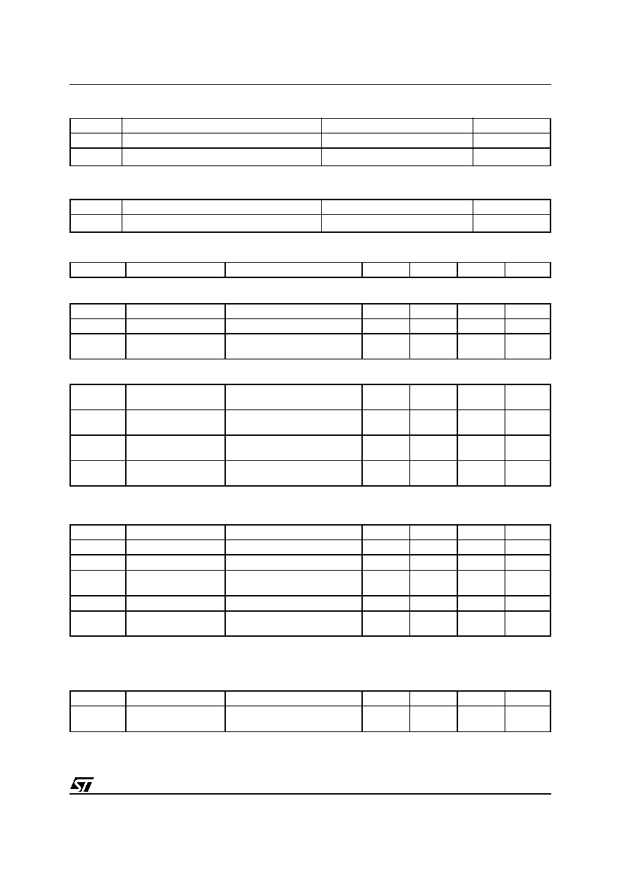
BLOCK DIAGRAM (GPS L1)
LNA section
The RF input signal is amplified by two gain levels
LNA. Using gain control pin the LNA gain is set to
19 dB to support passive antenna or 10 dB to sup-
port active antenna. The LNA output signal is fil-
tered by 1575.42 MHz SAW filter.
RF Amplifier plus mixer section
The 1575.42 MHz input signal, amplified by RF
amp., is mixed with the VCO signal to generate a
differential 20.46MHz IF signal
IF section
Two LC filters at mixer output and at first limiting
output are used to suppress undesirable signals
and mixer products. The second stage limiting
amplifier is connected to a D-Type latch clocked
by 16.368MHz crystal oscillator signal. The effect
of sampling the 20.46MHz signal at 16.368MHz is
to create sub-sampling alias at 4.092MHz. This is
fed to the output level converter.
Output section
The output buffers perform level translation from
the internal ECL levels to CMOS output levels re-
ferred to ground. The Data signal changes during
the clock signal negative edge.
Power supplies
The STB5610, has been designed to support
from 2.7 V to 3.6 V supply voltage.
VCO and PLL
Using external tank the VCO is able to provide
very low phase noise signal. Through the freq. se-
lector pin the VCO signal is set at 1554.96 MHz
and at 1571.328 MHz. The on-chip reference os-
cillator uses a low cost 16.368 MHz crystal.
Antenna sensor circuitry
Integrated sensor circuitry is able to evaluate the
antenna current consumption; the Asout pin out-
put provides this info externally. Using external
sensing resistor of 10 Ohm if the antenna current
consumption is inside the range 10mA...40mA
(active antennas typical current consumption) the
Asout output logic level is High, if the antenna cur-
rent consumption is outside the above reported
range (passive antenna or problem on antenna
connection) the Asout output logic level is low.
Chip enable
Using the CE pin it is possible to switch off all the
chip ( neither data nor clock available).
Using CE2 pin it is possible to disable the analog
portion of the chip (no data available) maintaining
the digital portion active (Clock available) optimiz-
ing the chip current consumption.
FUNCTIONAL DESCRIPTION
5/11
STB5610
ELECTRICAL CHARACTERISTICS (Vcc = 3+/-10%, Tcase= 25
o
C)
Symbol
Parameter
Test conditions
Min.
Typ.
Max.
Unit
ABSOLUTE MAXIMUM RATING
Symbol
Parameter
Value
Unit
Vcc
Supply voltage
5.9
V
Tj
Junction operating temperature
-40 to 125
o
C
THERMAL DATA
Symbol
Parameter
Value
Unit
Rthj-case
Thermal resistance junction-case
TBD
o
C/W
SUPPLY
Vcc
Supply voltage
2.7
3.3
3.6
V
Icc
Supply current
37
mA
AS1
Vcc Antenna
Supply
2.7
3.3 / 5
5.5
V
LNA
Gp
Power gain
Pin GC at GND
Pin GC at Vcc
19
10
dB
NF
Noise figure
Pin GC at GND
Pin GC at Vcc
3
10
dB
IIP3
Input IP3
Pin GC at GND
Pin GC at Vcc
-20
-5
dBm
VSWRin
Voltage Stat. Wave
Ratio
Z
L
=50
2.1
RF AMPLIFIER AND MIXER
CHAIN
IIP3
Input IP3
-19
dBm
NF
Noise Figure
5.5
dB
Z
IN
Input impedance
50
Z
OUT
Differential output
impedance
1.4
fRF
Input signal RF
1.575
MHz
G
Voltage Convertion
Gain
30
dB
FIRST LIMITING AMPLIFIER
G
Voltage Gain
60
dB
Z
OUT
Differential output
impedance
2.4