Äîêóìåíòàöèÿ è îïèñàíèÿ www.docs.chipfind.ru
STB60NF03L
N-CHANNEL 30V - 0.008
- 60A D
2
PAK
STripFET
TM
POWER MOSFET
PRELIMINARY DATA
s
TYPICAL R
DS(on)
= 0.008
s
OPTIMIMIZED FOR HIGH SWITCHING
OPERATIONS
s
LOW THRESHOLD DRIVE
s
LOGIC LEVEL GATE DRIVE
DESCRIPTION
This Power Mosfet is the latest development of
STMicroelectronics
unique
"Single
Feature
Size
TM
"
strip-based
process.
The
resulting
transistor shows extremely high packing density
for
low
on-resistance,
rugged
avalance
characteristics and less critical alignment steps
therefore
a
remarkable
manufacturing
reproducibility.
APPLICATIONS
s
LOW VOLTAGE DC-DC CONVERTERS
s
HIGH CURRENT, HIGH SPEED SWITCHING
s
HIGH EFFICIENCY SWITCHING CIRCUITS
®
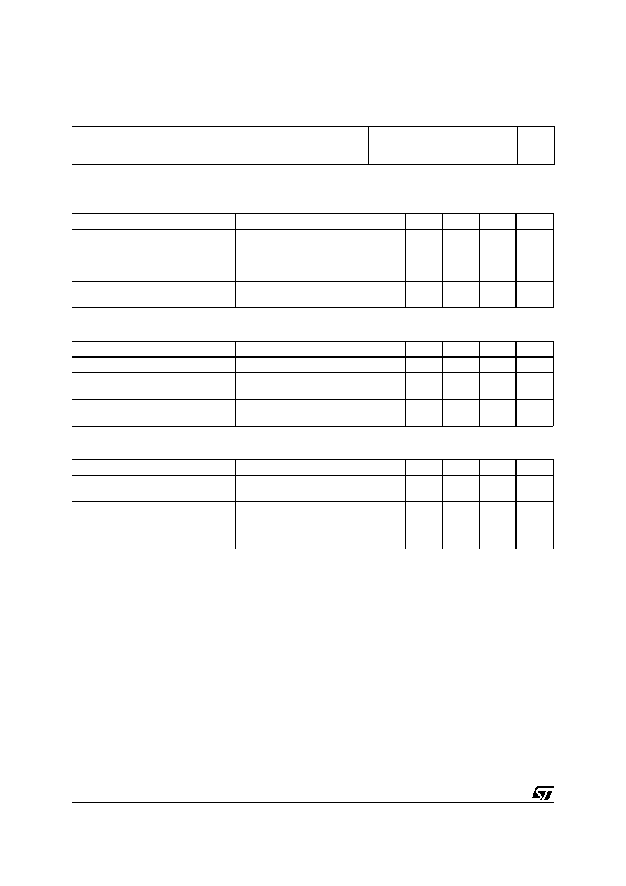
INTERNAL SCHEMATIC DIAGRAM
September 1999
1
3
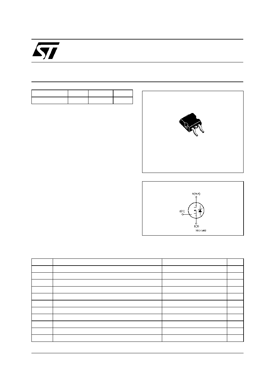
D
2
PAK
TO-263
ABSOLUTE MAXIMUM RATINGS
Symbol
Parameter
Value
Un it
V
DS
Drain-source Voltage (V
GS
= 0)
30
V
V
DGR
Drain- gate Voltage (R
GS
= 20 k
)
30
V
V
GS
G ate-source Volt age
±
20
V
I
D
Drain Current (continuous) at T
c
= 25
o
C
60
A
I
D
Drain Current (continuous) at T
c
= 100
o
C
42
A
I
DM
(
·
)
Drain Current (pulsed)
240
A
P
tot
T otal Dissipat ion at T
c
= 25
o
C
100
W
Derating Factor
0.67
W /
o
C
E
AS
(
1
)
Single Pulse Avalanche Energy
650
mJ
T
s tg
Storage Temperature
-65 to 175
o
C
T
j
Max. Operating Junction Temperature
175
o
C
(
·
) Pulse width limited by safe operating area
(
1
)
starting T
j
= 25
o
C, I
D
= 30A , V
DD
= 20V
T YPE
V
DSS
R
DS(on)
I
D
STB60NF03L
30 V
< 0. 01
60 A
ADD SUFFIX "T4" FOR ORDERING IN TAPE & REEL
1/6
THERMAL DATA
R
thj -case
R
thj -amb
T
l
Thermal Resistance Junction-case
Max
Thermal Resistance Junction-ambient
Max
Maximum Lead Temperature F or Soldering Purpose
1.5
62.5
300
o
C/W
o
C/W
o
C
ELECTRICAL CHARACTERISTICS (T
case
= 25
o
C unless otherwise specified)
OFF
Symbo l
Parameter
Test Con ditions
Min.
Typ.
Max.
Unit
V
(BR)DSS
Drain-source
Breakdown Voltage
I
D
= 250
µ
A
V
GS
= 0
30
V
I
DSS
Zero Gat e Voltage
Drain Current (V
GS
= 0)
V
DS
= Max Rat ing
V
DS
= Max Rat ing
T
c
=125
o
C
1
10
µ
A
µ
A
I
G SS
Gat e-body Leakage
Current (V
DS
= 0)
V
GS
=
±
20 V
±
100
nA
ON (
)
Symbo l
Parameter
Test Con ditions
Min.
Typ.
Max.
Unit
V
G S(th)
Gat e Threshold Voltage V
DS
= V
GS
I
D
= 250
µ
A
1
1.5
2. 5
V
R
DS(on)
Static Drain-source On
Resistance
V
GS
= 10V
I
D
= 30 A
V
GS
= 4. 5V
I
D
= 30 A
0.008
0.0095
0.01
0.015
I
D(o n)
On State Drain Current
V
DS
> I
D(o n)
x R
DS(on )ma x
V
GS
= 10 V
60
A
DYNAMIC
Symbo l
Parameter
Test Con ditions
Min.
Typ.
Max.
Unit
g
f s
(
)
Forward
Transconductance
V
DS
> I
D(o n)
x R
DS(on )ma x
I
D
=30 A
60
S
C
iss
C
os s
C
rss
Input Capacitance
Out put Capacitance
Reverse Transfer
Capacitance
V
DS
= 25 V
f = 1 MHz
V
GS
= 0
2550
630
215
pF
pF
pF
STB60NF03L
2/6
ELECTRICAL CHARACTERISTICS (continued)
SWITCHING ON
Symbo l
Parameter
Test Con ditions
Min.
Typ.
Max.
Unit
t
d(on)
t
r
Turn-on Delay T ime
Rise Time
V
DD
= 15 V
I
D
= 30 A
R
G
= 4.7
V
G S
= 4.5 V
(Resistive Load, see fig. 3)
40
250
ns
ns
Q
g
Q
gs
Q
gd
Tot al G ate Charge
Gat e-Source Charge
Gat e-Drain Charge
V
DD
= 24 V I
D
= 60 A V
GS
= 5 V
43
12
21
58
nC
nC
nC
SWITCHING OFF
Symbo l
Parameter
Test Con ditions
Min.
Typ.
Max.
Unit
t
d(of f)
t
f
Turn-off Delay T ime
Fall T ime
V
DD
= 15 V
I
D
= 30 A
R
G
= 4.7
V
G S
= 4.5 V
(Resistive Load, see fig. 3)
60
70
ns
ns
SOURCE DRAIN DIODE
Symbo l
Parameter
Test Con ditions
Min.
Typ.
Max.
Unit
I
SD
I
SDM
(
·
)
Source-drain Current
Source-drain Current
(pulsed)
60
240
A
A
V
SD
(
)
Forward On Voltage
I
SD
= 60 A
V
GS
= 0
1. 5
V
t
rr
Q
rr
I
RRM
Reverse Recovery
Time
Reverse Recovery
Charge
Reverse Recovery
Current
I
SD
= 60 A
di/dt = 100 A/
µ
s
V
DD
= 15 V
T
j
= 150
o
C
(see t est circuit, f ig. 5)
75
100
2.6
ns
nC
A
(
) Pulsed: Pulse duration = 300
µ
s, duty cycle 1.5 %
(
·
) Pulse width limited by safe operating area
STB60NF03L
3/6
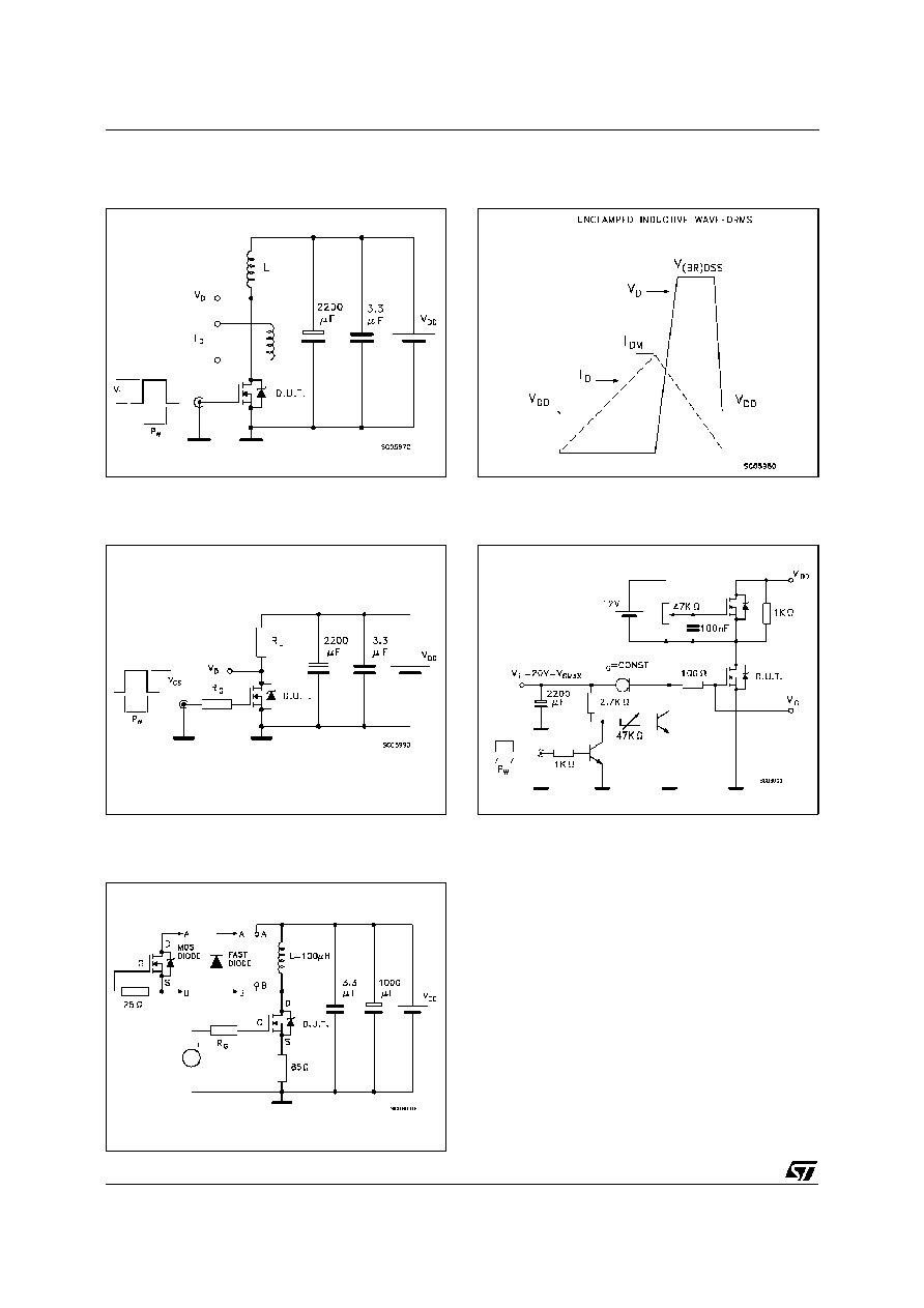
Fig. 1: Unclamped Inductive Load Test Circuit
Fig. 3: Switching Times Test Circuits For
Resistive Load
Fig. 2: Unclamped Inductive Waveform
Fig. 4: Gate Charge test Circuit
Fig. 5: Test Circuit For Inductive Load Switching
And Diode Recovery Times
STB60NF03L
4/6
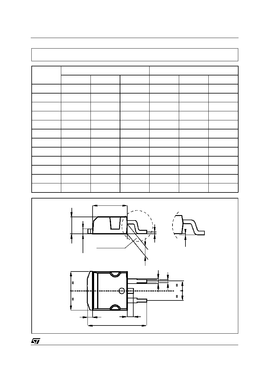
DIM.
mm
inch
MIN.
TYP.
MAX.
MIN.
TYP.
MAX.
A
4.4
4.6
0.173
0.181
A1
2.49
2.69
0.098
0.106
B
0.7
0.93
0.027
0.036
B2
1.14
1.7
0.044
0.067
C
0.45
0.6
0.017
0.023
C2
1.21
1.36
0.047
0.053
D
8.95
9.35
0.352
0.368
E
10
10.4
0.393
0.409
G
4.88
5.28
0.192
0.208
L
15
15.85
0.590
0.624
L2
1.27
1.4
0.050
0.055
L3
1.4
1.75
0.055
0.068
L2
L3
L
B2
B
G
E
A
C2
D
C
A1
DETAIL "A"
DETAIL "A"
A2
P011P6/E
TO-263 (D
2
PAK) MECHANICAL DATA
STB60NF03L
5/6