1/8
PRELIMINARY DATA
August 2004
STB7720L
2.4-2.5 GHz Silicon Linear Power Amplifier IC
REV. 1
Table 1. Order Codes
Table 2. Absolute Maximum Ratings (T
amb
= 25
o
C)
Table 3. Thermal Data
Order Codes
Marking
Package
Packaging
STB7720
7720
QFN16L (3x3)
Tape & Reel
Symbol
Parameter
Value
Unit
V
cc
Supply voltage
5.5
V
T
stb
Storage temperature
-55 to + 150
o
C
T
a
Operating Ambient Temperature
-30 + 85
o
C
P
in
Input Power
10
dBm
R
th(j-case)
Thermal Resistance Junction-Case
TBD
o
C/W
FEATURES SUMMARY
� EXCELLENT LINEARITY EVM 2% @ 19dBm (WITH
802.11g OFDM 54Mb/s MODULATION)
� VERY LOW QUIESCENT CURRENT (60mA)
� INTEGRATED LINEAR ANALOG CONTROL FOR
DC CURRENT AND OUTPUT MANAGEMENT
� INTEGRATED AVERAGE CHANNEL POWER
DETECTOR
� LEADLESS PACKAGE (3mmx3mm LEAD FREE)
APPLICATIONS
� OPTIMIZED FOR USE IN 802.11 b/g
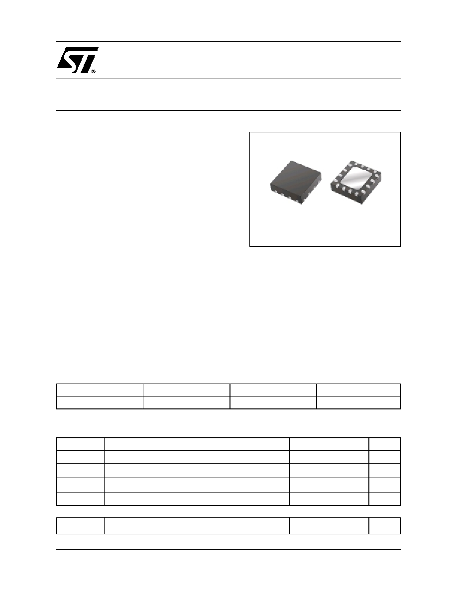
QFN16L (3x3)
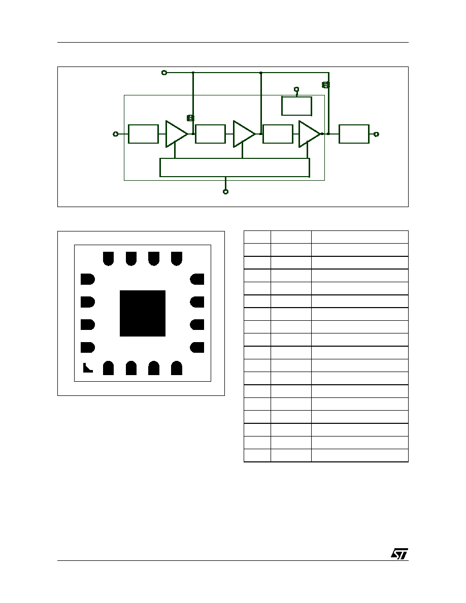
DESCRIPTION
The STB7720L, manufactured in the third generation of ST proprietary pure Si bipolar process, is a
three-stage linear power amplifier (PA) optimized for 802.11b/g wireless LAN (WLAN) applications in the
2.4GHz ISM band. It features 32dB of power gain and delivers 19dBm of linear output power with an EVM
degradation of only 2% under 802.11g Modulation (54Mbps).
The current consumption is as low as 125mA at 19dBm make the STB7720L a good solution for mobile
applications. It achieves less than -40dBc firstside lobe suppression and less than -52dBc secondside
lobe suppression under 802.11b modulation (11Mbps).
The device embeds a Linear Analog Control for DC current and output management and a Proprietary
Average Channel Power Detector solution. This power detector has 20dB dynamic range with 1 voltage
range and �0.3dB accuracy under 2:1 load mismatch. It provides a buffered DC voltage proportional to
the average channel output power. Thanks to this solution we save cost and space by removing a coupler,
an op amp (usually required in a power down function) and also an integrator.
The SBT7720 is housed in QFN 3mmx3mm Leadless package.
Figure 1. Package

3/8
STB7720L
Table 5. Electrical Characteristics (T
amd
= 25
o
C, V
cc
=3.3V, f=2.45GHz, Vcnt = 2.9V)
Notes:
(1) Parameter measured with RF modulation based on IEEE 802.11g standard (OFDM 54Mbps)
(2) Parameter measured with RF modulation based on IEEE 802.11b standard (CCK 11Mbps)
(3) Load VSWR is set to 10:1 and the angle is varied 360 degrees. Pout = -30 dBm to P1dB
(4) Measured from Device On signal turn on to the point where RF Pout stabilizes to 0.5dB
Symbol
Parameter
Test Conditions
Min.
Typ.
Max.
Unit
f
Frequency
2.4
2.45
2.5
GHz
V
cc
Supply Voltage
3.0
3.3
3.6
V
Icc
(1)
Current Consumption
P
out
= 19 dBm
125
mA
Gp
Power Gain
32
dB
P
1dB
P1dB Compression
25
dBm
Gain variation over
Frequency
-/+ 0.5
dB
Gain variation over
Temperature
-/+ 0.5
dB
Quiescent Current
60
mA
EVM
(1)
Error Vector Magnitude
P
out
= 19 dBm
2
%
ACPR
(2)
Adiacent Channel
Power Ratio
P
out
= 19dBm, 1st Side Lobe
P
out
= 19dBm, 2nd Side Lobe
-40
-52
dBc
dBc
V
det
Output Detector Voltage
Range
1
V
Output Detector Voltage
Response Time
4
�
s
2nd to 5th Harmonics
-40
dBc
Spurious (stability)
(3)
Load VSWR 10:1
-65
dBc
Turn On Time
(4)
0.5
�
s
STB7720L
4/8
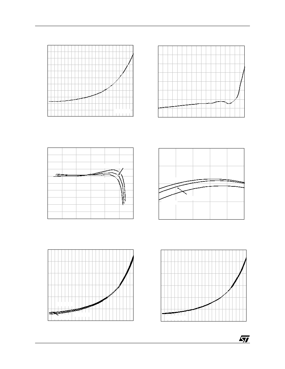
Figure 4. Supply Current Vs Output Power
0
25
50
75
100
125
150
175
200
225
250
275
0
5
10
15
20
25
Pout (dBm)
Ic
(m
A
)
Tc = +25 �C
TYPICAL PERFORMANCE
Figure 5. EVM Vs Output Power
0
1
2
3
4
5
6
7
8
3
5
7
9
11
13
15
17
19
21
Pout (dBm)
EVM
(%
)
Figure 6. Power Gain Vs Output Power
20
22
24
26
28
30
32
34
36
38
40
0
5
10
15
20
25
30
Pout (dBm)
Ga
i
n
(
d
B
)
Tc = -30 �C
Tc =+85 �C
Tc =+25 �C
Temp. depend.
Figure 7. Power Gain Vs Frequency
30
31
32
33
34
2400
2420
2440
2460
2480
2500
f (MHz)
Ga
i
n
(
d
B
)
Tc = -30 �C
Tc =+25 �C
Tc =+85 �C
Temp. depend.
Figure 8. Power Detector Voltage Vs Pout
400
600
800
1000
1200
1400
1600
0
5
10
15
20
25
Pout (dBm)
Vd
e
t
(
m
V)
Tc = -30 �C
Tc = +85 �C
Tc = +25 �C
Temp. depend.
Figure 9. Power Detector Voltage Vs Pout
400
600
800
1000
1200
1400
1600
0
5
10
15
20
25
Pout (dBm)
V
det
(
m
V
)
@ 3V, 3.3V, 3.6V
Vcc. depend.