1/9
November 2001
STB85NF3LL
N-CHANNEL 30V - 0.006
- 85A D
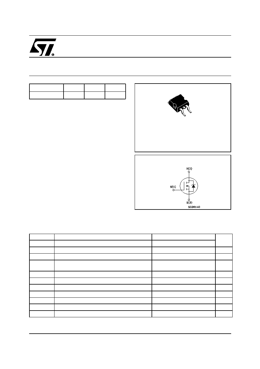
2
PAK
LOW GATE CHARGE STripFETTMII POWER MOSFET
s
TYPICAL R
DS
(on) = 0.0075
(@4.5V)
s
OPTIMAL R
DS
(on) x Qg TRADE-OFF @4.5V
s
CONDUCTION LOSSES REDUCED
s
SWITCHING LOSSES REDUCED
s
ADD SUFFIX "T4" FOR ORDERING IN TAPE &
REEL
DESCRIPTION
This application specific Power MOSFET is the third
genaration of STMicroelectronics unique " Single
Feature Size" strip-based process. The resulting
transistor shows the best trade-off between on-re-
sistance and gate charge. When used as high and
low side in buck regulators, it gives the best perfor-
mance in terms of both conduction and switching
losses. This is extremely important for mother-
boards where fast switching and high efficiency are
of paramount importance.
APPLICATIONS
s
SPECIFICALLY DESIGNED AND OPTIMISED
FOR HIGH EFFICIENCY CPU CORE DC/DC
CONVERTERS
ABSOLUTE MAXIMUM RATINGS
(
q
) Pulse width limited by safe operating area
TYPE
V
DSS
R
DS(on)
I
D
STB85NF3LL
30 V
< 0.008
85 A
Symbol
Parameter
Value
Unit
V
DS
Drain-source Voltage (V
GS
= 0)
30
V
V
DGR
Drain-gate Voltage (R
GS
= 20 k
)
30
V
V
GS
Gate- source Voltage
± 16
V
V
GSM
Gate-source Voltage Pulsed
(t
p
50
µ
s; duty cycle 25%; T
j
150∞C)
± 20
V
I
D
Drain Current (continuos) at T
C
= 25∞C
85
A
I
D
Drain Current (continuos) at T
C
= 100∞C
60
A
I
DM
(
l
)
Drain Current (pulsed)
340
A
P
TOT
Total Dissipation at T
C
= 25∞C
110
W
Derating Factor
0.73
W/∞C
T
stg
Storage Temperature
≠65 to 175
∞C
T
j
Max. Operating Junction Temperature
175
∞C
D
2
PAK
1
3
INTERNAL SCHEMATIC DIAGRAM
STB85NF3LL
2/9
THERMAL DATA
ELECTRICAL CHARACTERISTICS (TCASE = 25 ∞C UNLESS OTHERWISE SPECIFIED)
OFF
ON
(1)
DYNAMIC
Rthj-case
Thermal Resistance Junction-case Max
1.36
∞C/W
Rthj-amb
Thermal Resistance Junction-ambient Max
62.5
∞C/W
T
l
Maximum Lead Temperature For Soldering Purpose
300
∞C
Symbol
Parameter
Test Conditions
Min.
Typ.
Max.
Unit
V
(BR)DSS
Drain-source
Breakdown Voltage
I
D
= 250 µA, V
GS
= 0
30
V
I
DSS
Zero Gate Voltage
Drain Current (V
GS
= 0)
V
DS
= Max Rating
1
µA
V
DS
= Max Rating, T
C
= 125 ∞C
10
µA
I
GSS
Gate-body Leakage
Current (V
DS
= 0)
V
GS
= ± 16V
±100
nA
Symbol
Parameter
Test Conditions
Min.
Typ.
Max.
Unit
V
GS(th)
Gate Threshold Voltage
V
DS
= V
GS
, I
D
= 250µA
1
V
R
DS(on)
Static Drain-source On
Resistance
V
GS
= 10V, I
D
= 40 A
0.006
0.008
V
GS
= 4.5V, I
D
= 40 A
0.0075
0.0095
Symbol
Parameter
Test Conditions
Min.
Typ.
Max.
Unit
g
fs
(1)
Forward Transconductance
V
DS
> I
D(on)
x R
DS(on)max,
I
D
= 40 A
30
S
C
iss
Input Capacitance
V
DS
= 25V, f = 1 MHz, V
GS
= 0
2210
pF
C
oss
Output Capacitance
635
pF
C
rss
Reverse Transfer
Capacitance
138
pF
3/9
STB85NF3LL
ELECTRICAL CHARACTERISTICS (CONTINUED)
SWITCHING ON
SWITCHING OFF
SOURCE DRAIN DIODE
Note: 1. Pulsed: Pulse duration = 300 µs, duty cycle 1.5 %.
2. Pulse width limited by safe operating area.
Symbol
Parameter
Test Conditions
Min.
Typ.
Max.
Unit
t
d(on)
Turn-on Delay Time
V
DD
= 15V, I
D
= 30A
R
G
= 4.7
V
GS
= 4.5V
(see test circuit, Figure 3)
22
ns
t
r
Rise Time
130
ns
Q
g
Q
gs
Q
gd
Total Gate Charge
Gate-Source Charge
Gate-Drain Charge
V
DD
= 24V, I
D
= 60A,
V
GS
= 4.5V
30
9
12.5
40
nC
nC
nC
Symbol
Parameter
Test Conditions
Min.
Typ.
Max.
Unit
t
d(off)
t
f
Turn-off-Delay Time
Fall Time
V
DD
= 15V, I
D
= 30A,
R
G
= 4.7
,
V
GS
= 4.5V
(see test circuit, Figure 3)
36.5
36.5
ns
ns
t
d(off)
t
f
t
c
Off-voltage Rise Time
Fall Time
Cross-over Time
Vclamp =24V, I
D
=30A
R
G
= 4.7
,
V
GS
= 4.5V
(see test circuit, Figure 5)
32
23
40
ns
ns
ns
Symbol
Parameter
Test Conditions
Min.
Typ.
Max.
Unit
I
SD
Source-drain Current
85
A
I
SDM
(2)
Source-drain Current (pulsed)
340
A
V
SD
(1)
Forward On Voltage
I
SD
= 85A, V
GS
= 0
1.3
V
t
rr
Q
rr
I
RRM
Reverse Recovery Time
Reverse Recovery Charge
Reverse Recovery Current
I
SD
= 85A, di/dt = 100A/µs,
V
DD
= 15V, T
j
= 150∞C
(see test circuit, Figure 5)
65
105
3.4
ns
nC
A
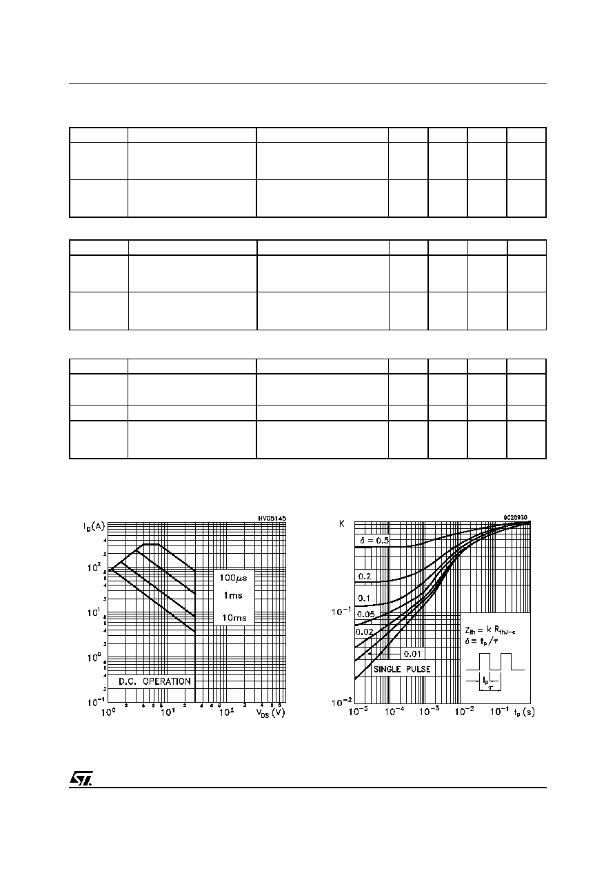
Thermal Impedence
Safe Operating Area
STB85NF3LL
4/9
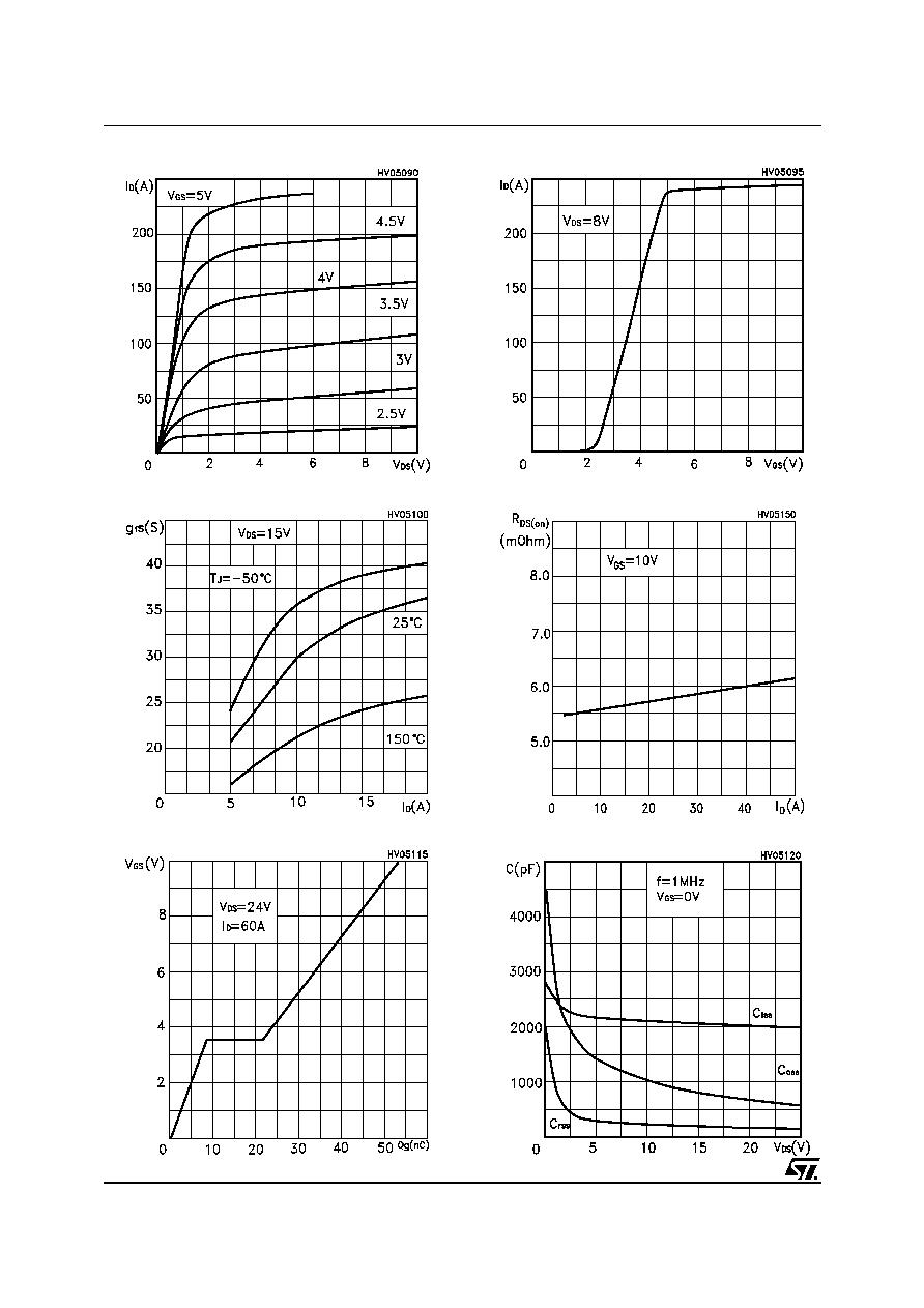
Transconductance
Output Characteristics
Gate Charge vs Gate-source Voltage
Capacitance Variations
Static Drain-source On Resistance
Transfer Characteristics
5/9
STB85NF3LL
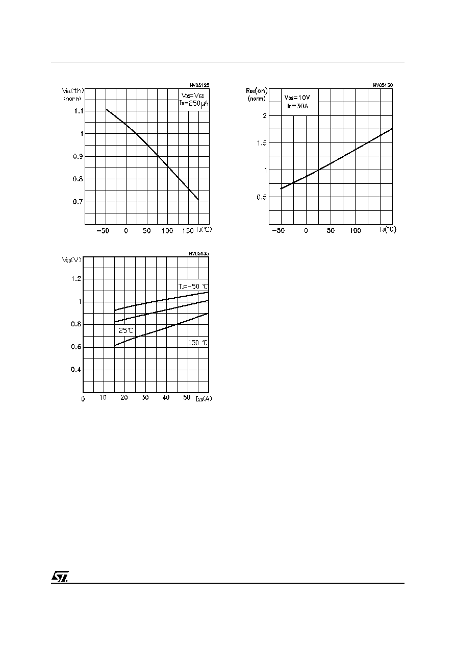
Source-drain Diode Forward Characteristics
Normalized On Resistance vs Temperature
Normalized Gate Thereshold Voltage vs Temp.