 | –≠–ª–µ–∫—Ç—Ä–æ–Ω–Ω—ã–π –∫–æ–º–ø–æ–Ω–µ–Ω—Ç: STBV32-AP | –°–∫–∞—á–∞—Ç—å:  PDF PDF  ZIP ZIP |
1/8
April 2003
STBV32
HIGH VOLTAGE FAST-SWITCHING
NPN POWER TRANSISTOR
n
HIGH VOLTAGE CAPABILITY
n
LOW SPREAD OF DYNAMIC PARAMETERS
n
MINIMUM LOT-TO-LOT SPREAD FOR
RELIABLE OPERATION
n
VERY HIGH SWITCHING SPEED
APPLICATIONS:
n
COMPACT FLUORESCENT LAMPS (CFLS)
DESCRIPTION
The device is manufactured using High Voltage
Multi Epitaxial Planar technology for high switching
speeds and high voltage capability.
It uses a Cellular Emitter structure with planar edge
termination to enhance switching speeds while
maintaining a wide RBSOA.
The STBV series is designed for use in Compact
Fluorescent Lamps.
ABSOLUTE MAXIMUM RATINGS
Ordering Code
Marking
Package / Shipment
STBV32
STBV32-AP
BV32
BV32
TO-92 / Bulk
TO-92 / Ammopack
Symbol
Parameter
Value
Unit
V
CES
Collector-Emitter Voltage (V
BE
= 0)
700
V
V
CEO
Collector-Emitter Voltage (I
B
= 0)
400
V
V
EBO
Emitter-Base Voltage (I
C
= 0, I
B
< 0.5 A, t
p
< 10 ms)
V
(BR)EBO
V
I
C
Collector Current
1
A
I
CM
Collector Peak Current (t
p
< 5 ms)
3
A
I
B
Base Current
0.5
A
I
BM
Base Peak Current (t
p
< 5 ms)
1.5
A
P
tot
Total Dissipation at T
amb
= 25 ∞C
1.1
W
T
stg
Storage Temperature
≠65 to 150
∞C
T
j
Max. Operating Junction Temperature
150
∞C
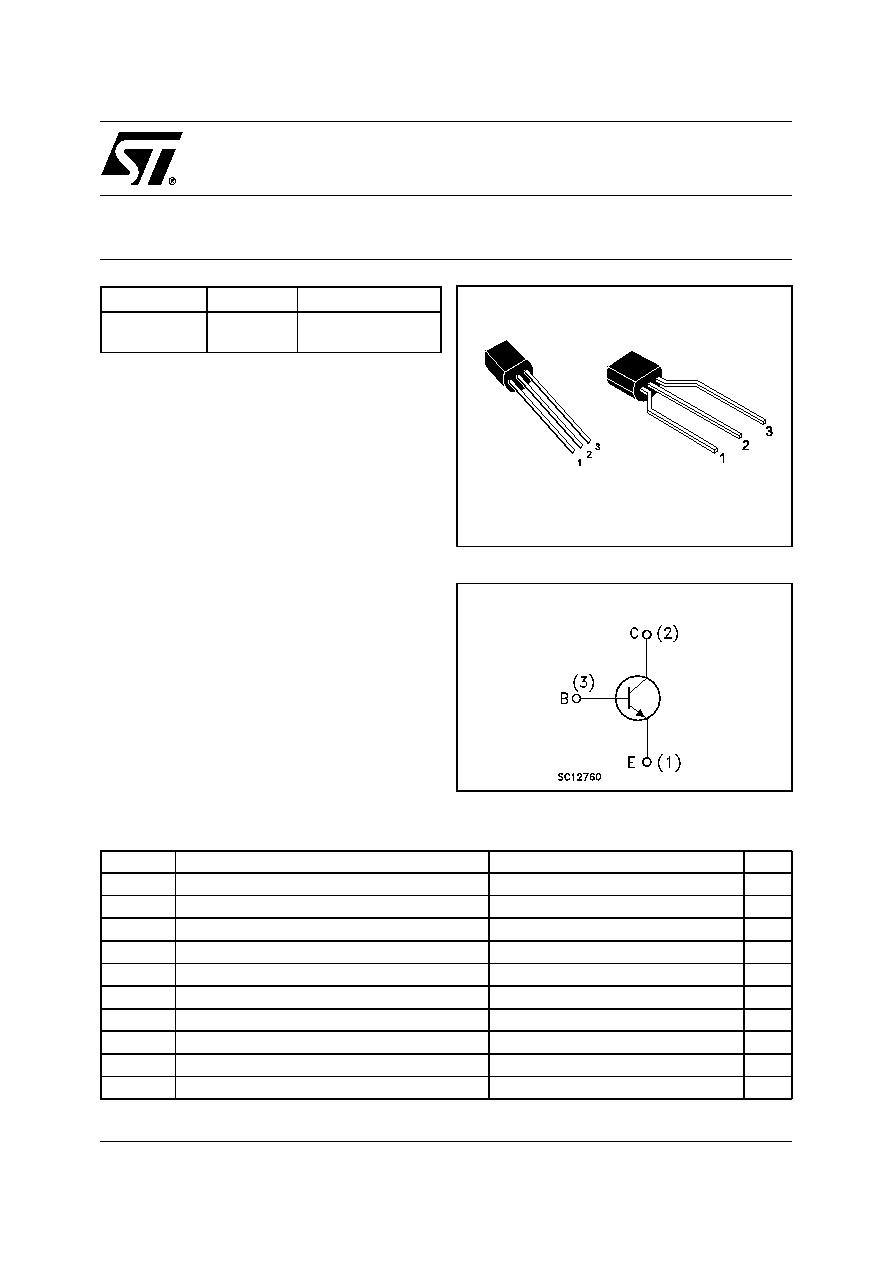
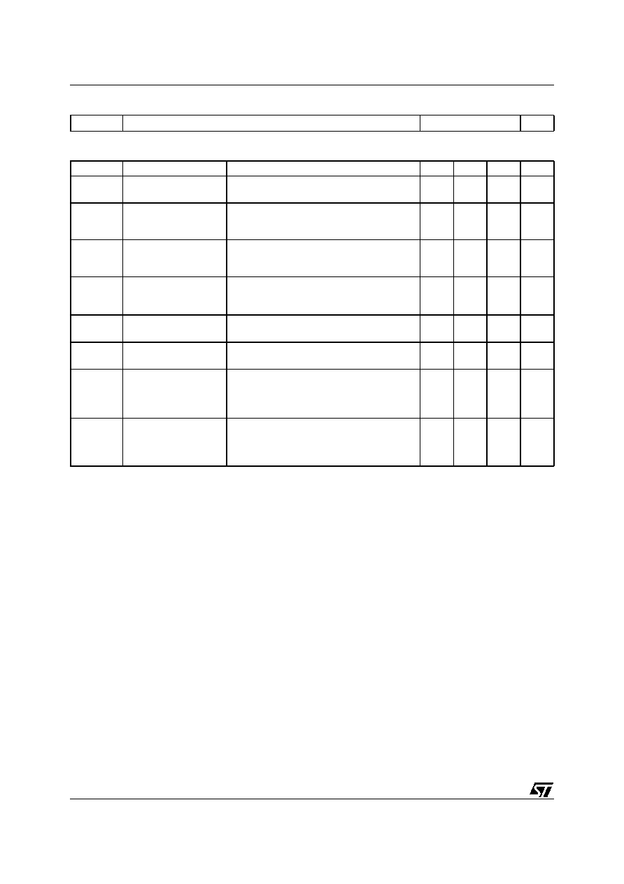
TO-92
TO-92
Bulk
Ammopack
INTERNAL SCHEMATIC DIAGRAM
STBV32
2/8
THERMAL DATA
ELECTRICAL CHARACTERISTICS (T
j
= 25 ∞C unless otherwise specified)
* Pulsed: Pulse duration = 300 µs, duty cycle = 1.5 %.
R
thj-amb
Thermal Resistance Junction-ambient
Max
112
∞C/W
Symbol
Parameter
Test Conditions
Min.
Typ.
Max.
Unit
I
CEV
Collector Cut-off
Current (V
BE
= -1.5 V)
V
CE
= 700 V
V
CE
= 700 V
T
j
= 125 ∞C
1
5
mA
mA
V
(BR)EBO
Emitter-Base
Breakdown Voltage
(I
C
= 0)
I
E
= 10 mA
9
18
V
V
CEO(sus)
*
Collector-Emitter
Sustaining Voltage
(I
B
= 0)
I
C
= 10 mA
400
V
V
CE(sat)
*
Collector-Emitter
Saturation Voltage
I
C
= 0.5 A
I
C
= 1 A
I
C
= 1.5 A
I
B
= 100 mA
I
B
= 250 mA
I
B
= 500 mA
0.5
1
1.5
V
V
V
V
BE(sat)
*
Base-Emitter
Saturation Voltage
I
C
= 0.5 A
I
C
= 1 A
I
B
= 100 mA
I
B
= 250 mA
1
1.2
V
V
h
FE
*
DC Current Gain
I
C
= 0.5 A
I
C
= 1 A
V
CE
= 2 V
V
CE
= 2 V
8
5
35
25
t
r
t
s
t
f
RESISTIVE LOAD
Rise Time
Storage Time
Fall Time
I
C
= 1 A
I
B1
= -I
B2
= 200 mA
(See Figure 1)
V
CC
= 125 V
t
p
= 25 µs
1
4
0.7
µs
µs
µs
t
s
INDUCTIVE LOAD
Storage Time
I
C
= 1 A
I
B1
= 200 mA
L = 50 mH
(See Figure 2)
V
clamp
= 300 V
V
BE(off)
= -5 V
R
BB
= 0
0.8
µs

3/8
STBV32
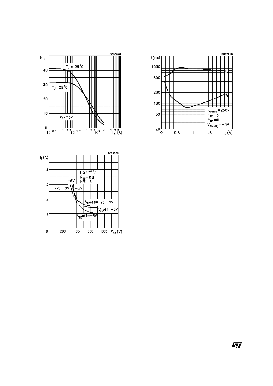
DC Current Gain
Base-Emitter Saturation Voltage
Collector-Emitter Saturation Voltage
Output characteristics
Safe Operating Area
Derating Curve
STBV32
4/8
DC Current Gain
Inductive Load Switching Times
Reverse Biased Safe Operating Area

5/8
STBV32
Figure 1: Resistive Load Switching Test Circuit
1) Fast Electronic Switch
2) Non-Inductive Resistor
Figure 2: Inductive Load Switching Test Circuit
1) Fast Electronic Switch
2) Non-Inductive Resistor
3) Fast Recovery Rectifier