 | –≠–ª–µ–∫—Ç—Ä–æ–Ω–Ω—ã–π –∫–æ–º–ø–æ–Ω–µ–Ω—Ç: STC2G15 | –°–∫–∞—á–∞—Ç—å:  PDF PDF  ZIP ZIP |
1/8
April 2003
s
INPUT VOLTAGE FROM 2.7V TO 5.02V
s
STABLE WITH LOW ESR CERAMIC AND
TANTALUM CAPACITORS
s
VERY LOW QUIESCENT CURRENT (30µA
TYP. AT NO LOAD; 2µA IN OFF MODE)
s
GUARANTEED OUTPUT CURRENT UP TO
15mA
s
OUTPUT VOLTAGE: 1.5V
s
LOGIC-CONTROLLED ELECTRONIC
SHUTDOWN
s
INTERNAL CURRENT LIMIT
s
JUNCTION TEMPERATURE RANGE: -40∞C
TO 95∞C
DESCRIPTION
The STC2G15 provides up to 15mA, from 2.5V to
6V input voltage. The low quiescent current
makes it suitable for low power applications and in
battery powered systems.
Shutdown Logic Control function is available, this
means that when the device is used as local
regulator, it is possible to put a part of the board in
standby, decreasing the total power consumption.
The STC2G15 is designed to work with low ESR
ceramic
and
tantalum
capacitors.
Typical
applications are in mobile phone, blue-tooth
module and similar battery powered wireless
systems.
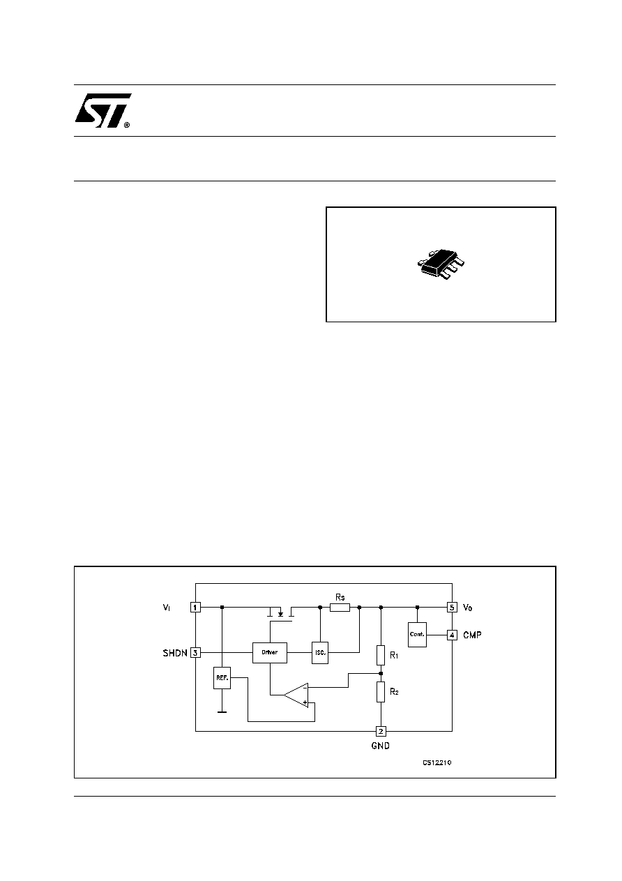
STC2G15
BCMOS VOLTAGE REGULATOR DESIGNED FOR USE WITH
VERY LOW ESR AND TANTALUM OUTPUT CAPACITOR
SCHEMATIC DIAGRAM
TSOT23-5L
STC2G15
2/8
ABSOLUTE MAXIMUM RATINGS
Absolute Maximum Ratings are those values beyond which damage to the device may occur. Functional operation under these condition is
not implied.
THERMAL DATA
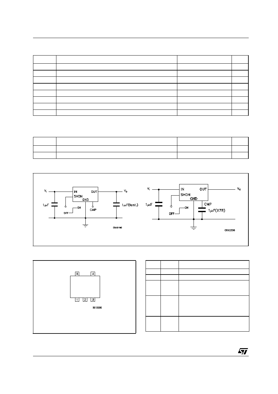
APPLICATION CIRCUITS
CONNECTION DIAGRAM (top view)
PIN DESCRIPTION
Symbol
Parameter
Value
Unit
V
I
DC Input Voltage
-0.3 to 5.4
V
V
O
DC Output Voltage
-0.3 to V
IN
+0.3
V
V
INH
INHIBIT Input Voltage
-0.3 to V
IN
+0.3
V
I
O
Output Current
Internally limited
P
tot
Power Dissipation
Internally limited
T
stg
Storage Temperature Range
-55 to +150
∞C
T
op
Operating Junction Temperature Range
-40 to +95
∞C
ESD
Electrostatic Discharge HBM (DH11C)
2
kV
Symbol
Parameter
TSOT23-5L
Unit
R
thj-amb
Thermal Resistance Junction-ambient
225
∞C/W
R
thj-case
Thermal Resistance Junction-case
81
∞C/W
Pin N∞ Symbol
Name and Function
1
IN
Input Pin
2
GND
Ground Pin
3
SHDN
Shutdown Input: Disables the
regulator when < 0.4V. Not internally
pulled down.
4
CMP
Compensation Pin: Bypass with a
1
µ
F ceramic X7R capacitor to GND
or leave floating if the C
O
is
connected to OUT pin
5
OUT
Output Pin: Bypass with a 1
µ
F
tantalium capacitor to GND if ceramic
X7R capacitoror is not used.
STC2G15
3/8
ORDERING CODES
ELECTRICAL CHARACTERISTICS (C
I
= 1
µ
F, C
O
= 1
µ
F (tantalium connected between OUT pin and
GND pin) or C
CMP
= 1
µ
F (ceramic X7R connected between CMP pin and GND pin) (unless otherwise
specified)
Note 1:Time for the output Voltage to rise from 50% to 85% of nominal value.
Note 2: Time for the output Voltage to fall from 85% to 50 of nominal value.
Note 3: Regulator must be able to sustain Regulated Output Voltage without load.
Note 4: Parameters are uncritical as long as the output voltage stays within limits.
Note 5: A sudden voltage rise/drop of 500mV mustn't bring the output Voltage out of limits.
Note 6: Ceramic Capacitors can be used if connected between CMP pin and GNG, instead of V
OUT
pin and GND.
Note 8: Maximum and minimum values are guaranteed in full temperature range.
Note 9: Line transient is tested when the input voltage changes from 2.7 to 3.2V in 10µs in full load range.
Note 10: Line transient is tested when the input voltage changes from 3.2 to 2.7V in 10µs in full load range.
Note 11: Load transient is tested when the load changes from 0.1 to 15mA in 10µs in all the input range
Note 13: Response time is defined as the time form the load line step until the output reaches a value within specification (1.41V, 1.59V).
Note 14: The maximum power dissipation for the operation depends on the ambient temperature.
For T
J
=95∞C, T
A
=85∞C and R
TJA
=220∞C/W the maximum power can be 0.045W. The maximum power dissipation for operation can be
increased by 4.5mW each degree below T
A
=85∞C, and it must be derated by 4.5mW for each degree above 85∞C
TYPE
TSOT23-5L
OUTPUT VOLTAGES
STC2G15
STC2G15R
1.5V
Symbol
Parameter
Test Conditions
Min.
Typ.
Max.
Unit
V
I
Input Voltage
2.7
5.2
V
V
O
Output Voltage
V
I
= 2.7 to 5.2V
I
O
= 0 to 15mA
T
J
= -40 to 95
∞C
1.41
1.5
1.59
V
t
RU
Output Voltage Ramp-Up
Time (Note 1)
I
O
= 0 to 15mA
10
15
µ
s
t
RD
Output Voltage Ramp-Down
Time (Note 2)
I
O
= 0 to 15mA
10
15
µ
s
I
O
Current Capability
15
mA
I
min
Minimum Load Current
(Note 3)
0
mA
Load Regulation (Note 4)
350
µ
V/mA
Temperature Drift (Note 4)
100
µ
V/K
SVR
Supply Voltage Rejection
(Note 5)
f = 1KHz
30
dB
I
d
Quiescent Current (ON
mode)
I
O
= 0
30
µ
A
I
O
= 0
V
I
= 2.7 to 5.2V
60
µ
A
I
d
Quiescent Current (OFF
mode)
2
4
µ
A
I
SHDN
Shutdown Pin Current
2
4
µ
A
V
SHDN
Shutdown Logic Enable
Low
0.4
V
V
SHDN
Shutdown Logic Disabled
High
1.15
V
Line Transient Response
Time (Notes 9, 13)
40
µ
s
Load Transient Response
Time (Notes 10, 13)
50
µ
s
Line Transient Response
Peak + (Notes 9)
80
mV
Line Transient Response
Peak - (Notes 10)
60
mV
Load Transient Response
Peak (Notes 11)
50
mV
eN
Output Noise Voltage
B= 1kHz to 1MHz
C
O
= 1
µ
F
10
mV
STC2G15
4/8
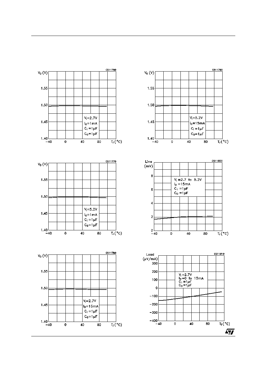
TYPICAL PERFORMANCE CHARACTERISTICS (unless otherwise specified C
IN
= C
COMP
= SMD X5R
C
OUT
= Tant., T
j
= 25∞C)
Figure 1 : Output Voltage vs Temperature
Figure 2 : Output Voltage vs Temperature
Figure 3 : Output Voltage vs Temperature
Figure 4 : Output Voltage vs Temperature
Figure 5 : Line Regulation vs Temperature
Figure 6 : Load Regulation vs Temperature
STC2G15
5/8
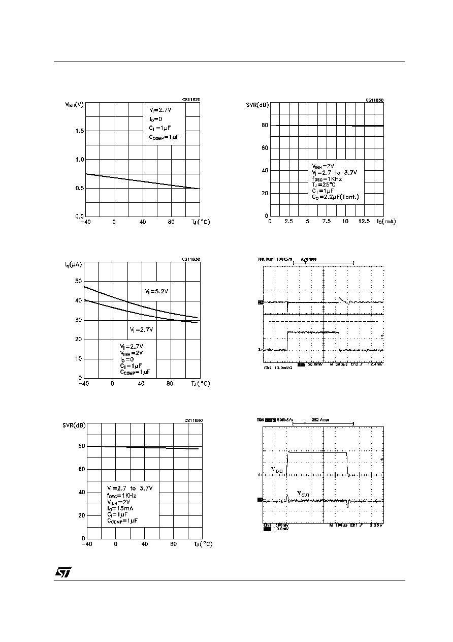
Figure 7 : Inhibit Threshold Voltage vs
Temperature
Figure 8 : Quiescent Current vs Temperature
Figure 9 : Supply Voltage Rejection vs
Temperature
Figure 10 : Supply Voltage Rejection vs Output
Current
Figure 11 : Dynamic Precharge Mode
Figure 12 : Dynamic Precharge Mode
V
I
=5V, I
O
=0.1 to 15mA, C
I
= 1
µ
FSMD X7R, C
O
=2.2
µ
F(tant)
V
I
=2.7 to 3.7V, I
O
=15mA, C
I
= 1
µ
FSMD X7R, C
O
=2.2
µ
F(tant),
t=1ms