 | ÐлекÑÑоннÑй компоненÑ: STCC02-E | СкаÑаÑÑ:  PDF PDF  ZIP ZIP |
Äîêóìåíòàöèÿ è îïèñàíèÿ www.docs.chipfind.ru

®
1/13
STCC02-ED5
CONTROL CIRCUIT FOR HOME APPLIANCE
MCU BASED APPLICATION
December 2004
REV. 1
APPLICATIONS
Microwaves oven analog and power driver control
Home Appliance digital control
FEATURES
Wide range input supply voltage operation:
7 to 27 V
5 V ± 10% full tolerance Voltage Regulator
MCU reset circuit with activation delay timer
and 45µs digital noise filter
Highly immune and 30 µs filtered Zero Voltage
Synchronization
Door Closed detection adaptation
One 100 mA fan relay coil driver with
demagnetizing diode
One 100 mA magnetron relay coil driver with
demagnetizing diode including down lock cir-
cuit based on fan drive output state
One 17 mA buzzer driver
Ambient temperature: - 10 to 80 °C
BENEFITS
Higher module compactness with reduced
component count
Drastic reduction of soldered pins on the board
for faster module assembly time and lower use
of lead
High ESD robustness and transient burst immu-
nity compliant with IEC61000-4 standards
Enhanced functional reliability
Accurate MCU supply for better Analog to Digi-
tal Conversion
Enhanced circuit parametric quality
Easy to design for short time to market
DIP-16
Figure 1: Pin Configuration (ball side)
V
IN
DL
C
SYN
DS
MAG
2
/RST
CDD
IN
3
BUZ
3
IN
1
IN
2
ZVS
V
DD
1
2
3
4
5
6
7
8
9
12
11
10
13
14
15
16
COM
V
CC
FAN
1
Table 1. Order Code
Part Number
Marking
STCC02-ED5
STCC02-E
STCC02-ED5
2/13
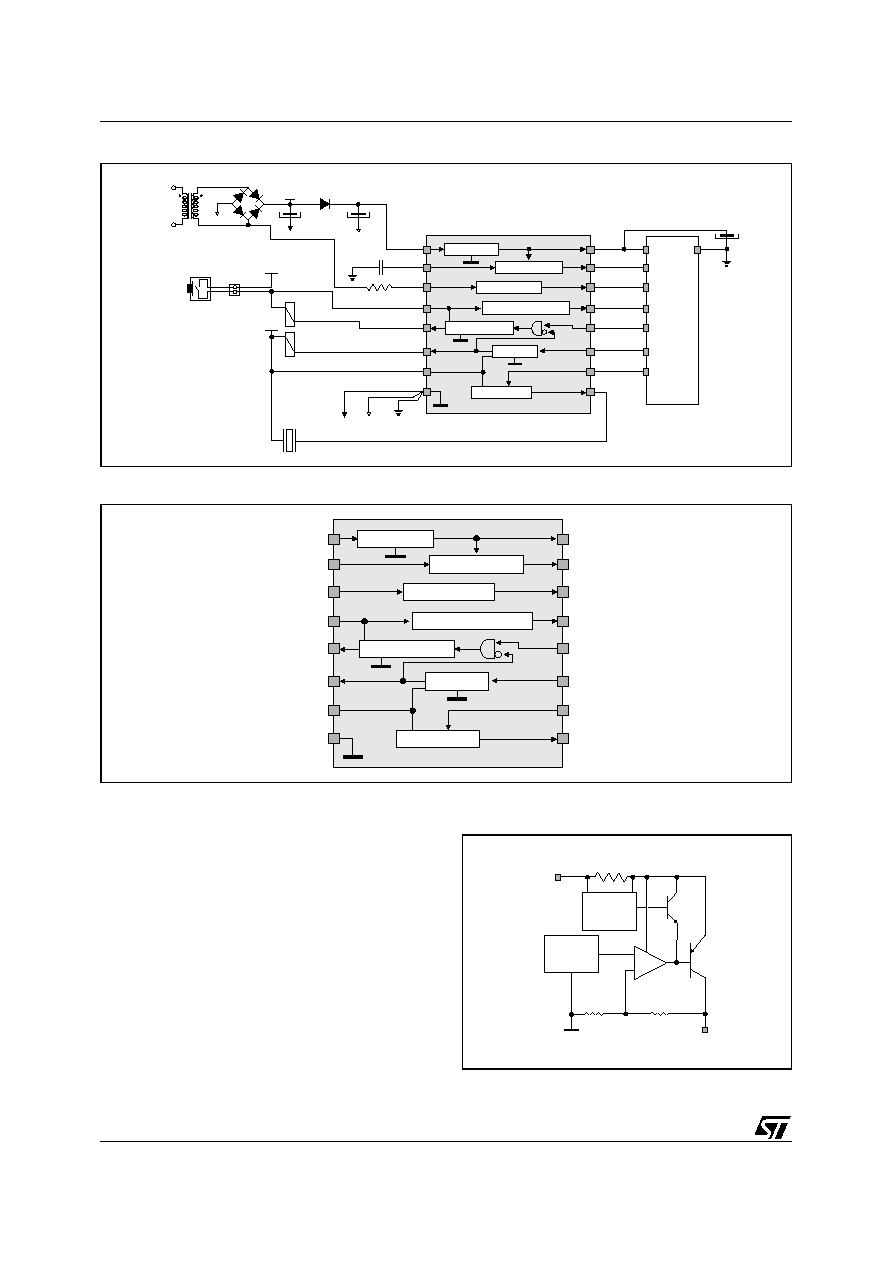
Figure 2: STCC02 Based Application Diagram
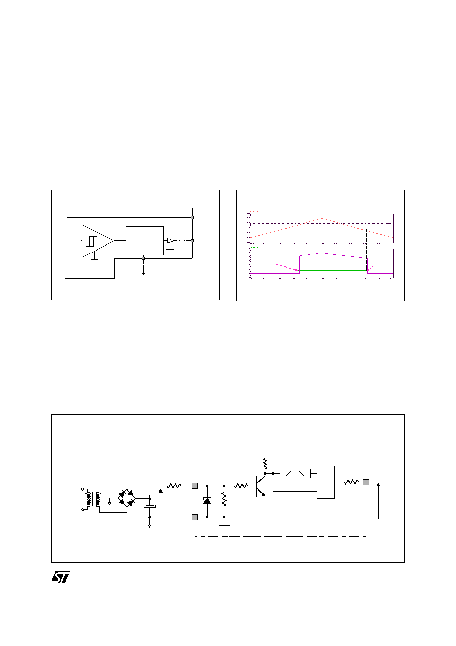
Figure 3: Circuit Block Diagram
FUNCTIONAL DESCRIPTION
The STCC02 is a control circuit embedding most of
the analog & power circuitry of a microwaves oven
control module. It interfaces the micro-controller with
the power and process sections of the oven.
The voltage supply
The 5V voltage regulator supplies the micro-control-
ler MCU: especially functions such as the timer, the
Analog-Digital Converter ADC, and the low current
outputs. Since all the high-current outputs sink their
current from a different voltage supply, this regula-
tor does not need to be oversized. Its average out-
put current can vary from 5 to 20 mA.
MCU
C
DD
C
DD
V
DD
V
IN
C
UP
V
IN
V
CC
V
CC
JP
V
CC
R
ZV
MAGNETRON RELAY
FAN RELAY
DOOR SWITCH
MAINS
Neutral
Line
BUZZER
/RST
DL
C
ZVS
SYN
C
DD
DS
IN
1
MAG
2
IN
2
FAN
1
IN
3
V
CC
BUZ
3
COM
/RST
NMI
P
03
P
02
P
01
P
04
V
SS
5V Regulator
Reset with delay
Zero volts sync.
Door closed detection
Magnetron driver
Fan driver
Buzzer driver
V
DD
V
IN
/RST
DL
C
ZVS
SYN
C
DD
DS
IN
1
MAG
2
IN
2
FAN
1
IN
3
V
CC
BUZ
3
COM
5V Regulator
Reset with delay
Zero volts sync.
Door closed detection
Magnetron driver
Fan driver
Buzzer driver
V
IN
Over current
limiter
1.25V
Reference
V
DD
R
1
-
+
R
2
R
SENSE
STCC02-ED5
3/13
Its output voltage accuracy, that contributes to the ADC accuracy of the MCU, is better than ± 10 % in the
whole operating range of the temperature T
AMB
, the load current I
DD
and the input voltage V
IN
. The
STCC02 input voltage range from 7 to 27 V; and its DC output current is less than 20 mA to keep the inter-
nal dissipation compatible with thermal package capability.
The regulator includes also an over current limiter to prevent high current conditions during the power up
inrush or the output short circuit. This limiter is made of a serial shunt resistance as current sensor and a
circuit that regulates the input over current.
The reset circuit
This circuit ensures a Low Voltage Detection (LVD) of the output voltage of the regulator. Most micro-
controllers have an active RESET pin in the low state: so, the /RST pin will be active at low state.
The reset circuit senses the regulator voltage V
DD
. Its comparator with hysteresis achieves this task.
The /RST pin is high when V
DD
is higher than the high threshold V
H
= 4.25 V; and is low when the V
DD
decreases below the low threshold V
L
= 3.75 V.
The comparator output changes are filtered for a high immunity. When the reset is disabling (V
DD
> V
H
),
the /RST signal rises after the delay time T
UP
. This delay is set by an external capacitor C
UP
connected
to the DL
C
pin: T
UP
= 6 ms for C
UP
= 47 nF.
When the reset is enabling (V
DD
< V
L
), the /RST signal is falling after a delay time T
DW
that is internally
set at 40
µs when C
UP
= 47 nF.
The Zero Voltage Synchronization ZVS Circuit
DL
C
If C
= 47 nF, T
= 6 ms
UP
UP
External
Capacitor
C
UP
/RST
PROGRAMMABLE
DELAY
NOISE FILTER
V
DD
V
DD
V
H
V = 4.25 V
H
500
V
L
V = 3.75 V
L
T
DW
~ 40 µs
V
DD
circuit output
internal latch output
T
UP
= 6 ms
C
UP
= 47 nF
RST\
T
DW
~ 40 µs
V
DD
circuit output
internal latch output
T
UP
= 6 ms
C
UP
= 47 nF
RST\
V
CC
V
DD
ZVS
V
ZVS
V
TF
COM
100 k
500
25 k
SYN
20 µs Filter
R
ZV
AC
LINE
Q
S
2
S
1
STCC02-ED5
4/13
The Zero Voltage Synchronization ZVS circuit generates a low frequency clock using the AC line cycles
(20 ms on 50 Hz or 16.7 ms on 60 Hz). This clock allows the MCU to generate the cooking timings and to
reduce the magnetron inrush current by powering it on at the AC line peak voltage.
The input pin SYN is an image of the mains voltage and is usually connected to the supply transformer
through a resistor R
ZV
.
The circuit is protected against fast line transients because its state change will act on the whole MCU
routines: a 30
µs filter is implemented giving a higher immunity to the MCU circuit.
Since the ZVS pin connected to the Non Maskable Interrupt NMI or INT\ of the MCU, its falling edge is the
active counting event. The delay between the real Zero Crossing event and this ZVS falling edge depends
on the internal filtering time, the resistance R
ZV
, the transformer, the rectifier drop voltage V
F
, the V
CC
sup-
ply load and the temperature. The STCC02 contribution to this delay can be evaluated by measuring the
delay between its input voltage V
TF
and its output voltage V
ZVS
. When using V
F
= 0.8V, R
ZV
= 10 k
, V
CC
= 15V, I
CC
= 20 mA, it is about 50
µs on rising voltage V
TF
and 115
µs on falling voltage V
TF
.
Door closed detection circuit
The magnetron of the oven can be powered only if the door is closed in order to protect the oven user.
This safety feature is ensured mechanically by putting the door switch in series with the magnetron relay
coil supply.
For redundancy purpose, the Door Closed Detection CDD signal is also transmitted to the MCU. Since the
DS input detects the door state from an electromechanical switch, a spike suppressor is added to increase
its robustness. Its EMI immunity in off state (open door) is increased thanks to a 50k
pull down resistor
that maintains the DS signal in low state. When DS is high (24V), CDD signal is also in high state (5V).
50µs
115µs
50µs
50µs
115µs
115µs
R
ZV
CC
CC
= 10 k ; V
= 15 V; I
= 20 mA
V
ZVS
FALLING EDGE
RISING EDGE
V
TF
2V / div
40µs / div
V
CC
V
DD
C
DD
DS
Door Switch
EMI Filter
500
V
DD
50 k
25 k

STCC02-ED5
5/13
The magnetron relay coil driver
This robust driver interfaces a DC relay coil and an MCU output. The relay coil power is rated up to 1.2 W
for V
CC
= 12V.
Its output stage is made of a transistor and a demagnetization diode. The transistor's reference is to the
power ground COM and has a DC current rating of 100 mA. Its collector is connected to the outputs MAG
2
.
The diode is connected between the output pin MAG
2
and the Door Switch pin DS.
To enhance safety rules and to prevent any unventilated operation of the magnetron, the relay coil mag-
netization is enabled by the fan conduction state that becomes a logic signal FAN
1
\.
Furthermore, its demagnetization node is connected to the door switch pin DS: when the oven door is
open, the coil of the magnetron relay is immediately disconnected from the relay supply V
CC
to switch off
these heating loads.
The boolean rule of the magnetron relay operation becomes:
(Magnetron relay ON) = DS.IN
2
.FAN
1
\.
Fan relay coil driver
This robust driver interfaces a DC relay coil and an MCU output. The relay coil power is rated up to 1.2W
for V
CC
=12 V.
Its output stage is made of a transistor and a demagnetization diode. The transistor is referred to the
ground COM, has a DC current rating of 100 mA; and its collector is connected to the output FAN
1
. The
diode is connected between the output pin FAN
1
and the supply pin V
CC
.
V
DD
MAG
2
IN
2
FAN
1
DS
Demagnetizing Diode
Relay
Transistor
15 k
V
CC
V
CC
V
DD
V
DD
BUZ
3
FAN
1
IN
3
IN
1
Relay
Transistor
Buzzer
Transistor
Demagnetizing Diode
50 k
15 k
1.5 k