Æ
1/13
STCC05-B
HOME APPLIANCE CONTROL CIRCUIT
October 2004
REV. 1
BUZZER
R
S
POWER RELAYS
COMPRESSOR RELAY
V
PS
MCU
/RS
T
P
02
P
03
P
01
NMI
V
DD
C
UP
PWM
P
06
P
07
C
DD
V
SS
V
DD
P
04
V
PS
AC Line
STCC05
V
PS
SMPS
SPEED
SENSOR
V
PS
JP
R
INS
BUZZER
DRIVER
V
PS
V
PS
V
PS
RELAY DRIVER
RELAY DRIVER
RELAY DRIVER
20A RELAY
DRIVER
V
PS
V
PS
5V REGULATOR
RESET
LEVEL SHIFTER
EMI FILTER
30µs FILTER
ZERO VOLTS SYNC.
V
PS
RST\
OUT
S
IN
BZ
IN
3
IN
4
IN
1
IN
2
ZVS
V
DD
EN
BZ
COM
BZ
1
V
PS
IN
S
SYN
RL
1
RL
2
RL
3
RL
4
BZ
2
V
PS
V
PS
V
PS
V
PS
V
PS
V
PS
V
PS
V
PS
V
PS
V
PS
V
PS
V
PS
V
PS
V
PS
V
PS
V
PS
V
PS
RST\
OUT
S
IN
BZ
IN
3
IN
4
IN
1
IN
2
ZVS
V
DD
EN
BZ
RST\
OUT
S
IN
BZ
IN
3
IN
4
IN
1
IN
2
ZVS
V
DD
EN
BZ
COM
BZ
1
V
PS
IN
S
SYN
RL
1
RL
2
RL
3
RL
4
BZ
2
COM
BZ
1
V
PS
IN
S
SYN
RL
1
RL
2
RL
3
RL
4
BZ
2
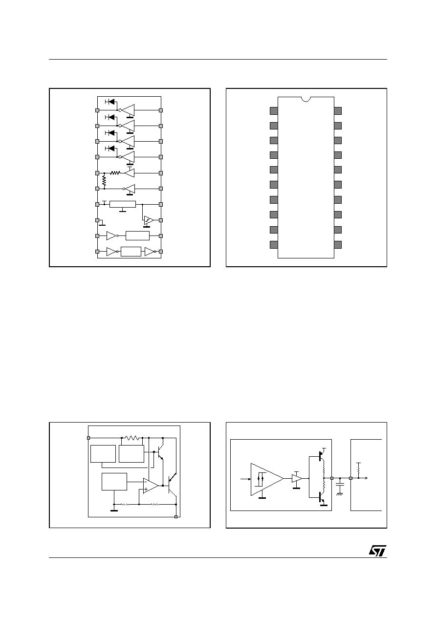
DIP-20
Table 1. Order Code
Part Number
Marking
STCC05-BD4
STCC05-B
APPLICATIONS
Home Appliance digital control
AC Power drive and functional safety management
Air Conditioner, Refrigerator and Oven applications
Compressor, fan, heater and valve drive circuit
FEATURES
Wide range input supply voltage operation:
7 to 18V
5 V +/- 5% full tolerance voltage regulator and
50mA output current
MCU reset circuit with activation delay time and
hysteresis (3.75V Hi, 3.4V Lo)
30µs digitally filtered inverting Zero Voltage
Synchronization
Three 50mA relay coil drivers with demagnetiz-
ing diode
BENEFITS
Higher module compactness with reduced component count
Drastic reduction of soldered pins on the board for lower use of lead metal
Faster module assembly time
High transient burst immunity and ESD robustness compliant with IEC61000-4 standards
Enhanced functional reliability
Enhanced circuit parametric quality
Easy to design for short time to market
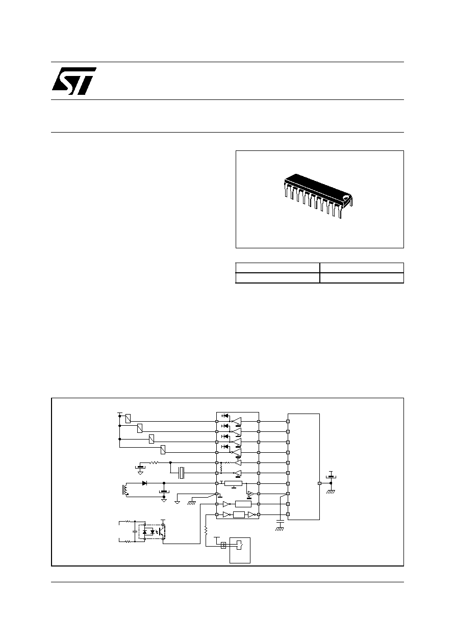
Figure 1: STCC05 based Air Conditioner application diagram
One 150mA relay coil driver with demagnetizing diode for a 20A relay
One 30mA peak enhanced buzzer driver with enable pin and soft turn off
12 to 5V robust non inverting level shifter for speed sensor or door switch interface
Ambient temperature: - 20 to 85∞C
STCC05-B
2/13
FUNCTIONAL DESCRIPTION
The STCC05 is a control circuit embedding most of the analog & power circuitry of an air conditioner or
refrigirator control module. It interfaces the micro-controller MCU with the AC power and cooling process
sections.
The voltage supply
The 5V voltage regulator supplies the micro-controller MCU. Its input voltage ranges from 7V to 18V; and
its average DC output current up to 50mA. With an output filtering capacitor of 100µF, its output voltage
accuracy is better than +/- 5% in the whole operating range of the ambient temperature T
AMB
, the load
current I
DD
and the input voltage V
PS
, contributing directly to the ADC accuracy.
The regulator includes also an over current limiter and a thermal shutdown. The over current limiter pro-
tects the regulator against output short circuits and inrush currents during the power up. The current limiter
is made of a serial shunt resistance as current sensor and a circuit that regulates the input current. More-
over, the thermal shutdown protects the whole circuit against overload operations. It is made of a thermal
sensing junction and a hysteresis comparator that is able to switch off the passing element.
Figure 2. Block diagram
Figure 3. Pin-out connections
RL
4
IN
4
IN
3
IN
2
IN
1
RL
3
RL
2
RL
1
BZ
2
EN
BZ
IN
BZ
V
DD
RST\
ZVS
BZ
1
VP
S
COM
SYN
IN
S
OUT
S
V
PS
20A RELAY
DRIVER
RELAY DRIVER
RELAY DRIVER
RELAY DRIVER
5V REGULATOR
BUZZER
DRIVER
V
PS
V
PS
V
PS
V
PS
V
PS
30µs FILTER
EMI FILTER
ZERO VOLTS SYNC.
RESET
LEVEL SHIFTER
V
PS
IN
S
RL
1
OUT
S
RL
2
RL
3
RL
4
BZ
1
BZ
2
EN
BZ
SYN
/RST
IN
3
IN
4
IN
BZ
COM
IN
1
IN
2
ZVS
V
DD
1
2
3
4
5
6
7
8
9
10
13
12
11
16
15
14
17
18
19
20
1.25 V
Reference
V
PS
V
DD
R
1
R
2
Over current
Limiter
R
SENSE
Thermal
Shutdown
V
H
= 3.75 V
V
L
= 3.40 V
V
DD
/RST
V
DD
V
H
V
L
C
UP
=
100nF
RESET
V
DD
3k
6k
V
DD
R
UP
> 100k
MCU
STCC05-B
3/13
The reset circuit
This circuit ensures a Low Voltage Detection (LVD) of the output of the regulator. Most micro-controllers
have an active RESET pin in the low state: so, the /RST pin will be active at low state.
The reset comparator senses the regulator voltage V
DD
. The /RST pin goes high when V
DD
is higher than
the high threshold V
H
= 3.75V and after a delay time T
UP
; and is low when the V
DD
decreases below the
low threshold V
L
= 3.4V after the delay time T
DW
.
These delays are set by an external capacitor C
UP
connected to the /RST pin and depend on the trigger
thresholds of /RST: For C
UP
= 100nF, T
UP
= 400µs with V
TH
= V
H
/2; T
DW
= 200µs with V
TH
= V
L
/2.
The Zero Voltage Synchronization ZVS circuit
The Zero Voltage Synchronization ZVS circuit generates the signal ZVS that synchronizes the whole oper-
ation with the AC line cycle (20 ms on 50 Hz or 16.7 ms on 60 Hz). This signal allows the MCU to control
the AC loads and achieve the timing functions.
The input pin SYN is an image of the mains voltage. It is connected to either the power supply transformer
through a resistor R
ZV
or an opto-coupler that is controlled directly by the AC line voltage. The circuit is
protected against fast line transient voltages: a robust ESD protection and a 30µs digital filter are imple-
mented to provide a higher immunity to the MCU operation. Its output signal ZVS is inverted respect to the
input signal V
SYN
.
The relay coil drivers
These robust circuits allow a DC relay coil to be driven by an MCU output. The relay coil has a minimum
resistance of 580
and has a power up to 0.25W for V
PS
= 12 V. These characteristics are representative
of 3A relays such as FTR-F3AA-12V or JQ1A-12V series.
The output stage is made of a transistor and a demagnetization diode. The transistor is referred to the
ground COM, has a DC current rating of 50mA; and its collector is connected to the output RL
I
(I=1, 2, 3).
The diode is connected between the output pin RL
I
and the supply pin V
PS
.
Moreover, a fourth coil driver has an extended 150mA current capability to be able to drive the coil of a
relay having a 130
minimum resistance and a 1.1W maximum power. These characteristics are repre-
sentative of 20A relays such as G4A-E-DC12, OMIF-S-112 or UKH12S series.
SYN
ZVS
V
DD
S
1
S
2
Q
30 µs FILTER
COM
70 k
25 k
30 k
STCC05-B
4/13
The buzzer driver with enable control
The MCU can excite a warning buzzer with a 50% PWM signal. The buzzer driver amplifies this signal in
current and translates it from the 5V MCU output to the V
PS
supply to produce the right sound level from
the buzzer.
The output stage is made of a NPN transistor, a PNP transistor and two 1k
resistors.
The NPN transistor, referred to the power ground COM, is controlled by the input IN
BZ
; its collector is con-
nected to the output BZ
1
. The input IN
BZ
is driven by a simple push-pull MCU buffer.
The PNP transistor, referred to the V
PS
polarity, is controlled by the input EN
BZ
; and its collector is con-
nected to the output BZ
2
through a 1k
resistor. The input EN
BZ
is driven by a simple push-pull MCU
buffer.
The pin BZ
2
is the supply terminal of the buzzer; and the circuit has a DC current rating of 9mA and the
PWM section runs from 10Hz up to 5kHz.
A 1k
resistor R
BZ
is connected between the BZ
1
and BZ
2
pins to discharge the buzzer periodically. More-
over, the addition of an external capacitor-resistor network on BZ
2
pin will allow the buzzer to turn on and
off smoothly when the pin EN
BZ
is toggling.
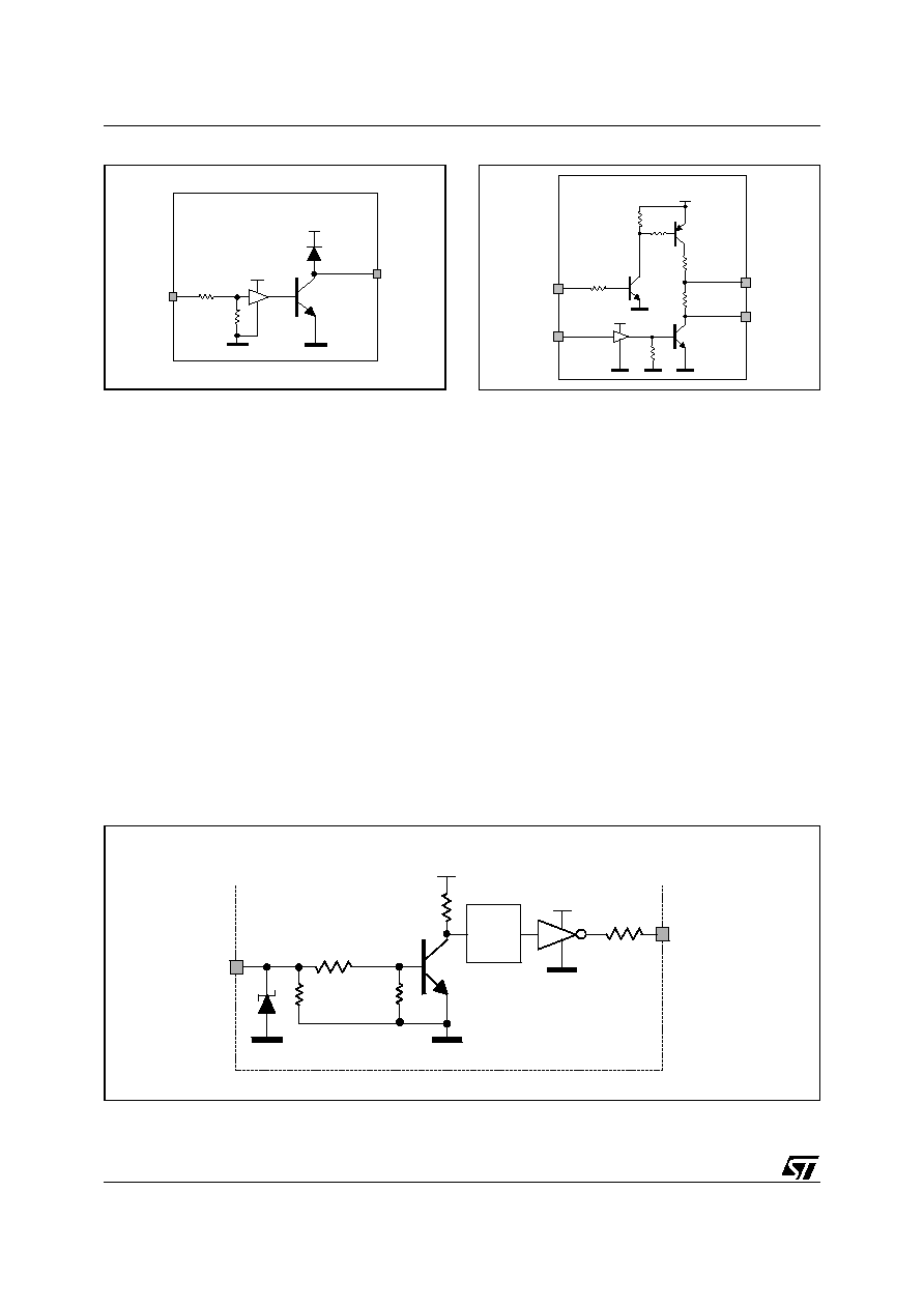
The speed sensor level shifter
The OUT
S
signal is generated by an electronic signal such as the indoor fan speed clock issued of a Hall
Effect sensor or a door switch signal and is transmitted to the MCU. As the IN
S
input may be disturbed; a
spike suppressor and a simple EMI filter are added to increase the input robustness. The output signal
OUT
S
is not inverted with respect to the input signal IN
S
.
Demagnetizing Diode
Relay
Transistor
V
PS
IN
I
RL
I
V
IN
10 k
4 k
BZ
1
BZ
2
V
PS
EN
BZ
IN
BZ
V
IN
R
OH
= 1k
R
BZ
=
1k
10 k
OUT
S
IN
S
V
DD
EMI
Filter
50 k
V
DD
500
50 k
50 k
STCC05-B
5/13
Table 2: Absolute Ratings (limiting values)
Table 3: Electromagnetic Compatibility Ratings
(T
J
= 25∞C, according to typical application diagram of page 1, unless otherwise specified)
Table 4: Thermal Resistance
Symbol
Pin
Parameter name & conditions
Value
Unit
V
DD
V
DD
Output supply voltage
- 0.3 to 6
V
V
PS
V
PS
, IN
S
Power supply voltage, level shifter input
- 0.3 to 20
V
V
SYN
SYN
ZVS input voltage, R
ZV
= 15k
- 1 to 20
V
V
MO
BZ
1
, BZ
2
,
RL
x
, x = 1 to 4
Output voltage
- 0.3 to
V
PS
+ 0.3
V
V
I
IN
1
, IN
2
, IN
3
Input logic voltage
- 0.3 to
V
DD
+ 0.3
V
V
O
ZVS,
OUT
S
, /RST
Output logic voltage
- 0.3 to
V
DD
+ 0.3
V
I
M
V
PS
Maximum sourced current pulse, tp = 10ms
500
mA
RL
x
, x = 1 to 3
Maximum sunk driver current pulse, tp = 10ms
60
mA
Maximum DC sunk current
50
mA
RL
4
Maximum sunk driver current pulse, tp = 10ms
160
mA
Maximum DC sunk current
150
mA
RL
x
, x = 1 to 4
Maximum diver diode reverse current
1
mA
I
BZ AV
BZ
1
, BZ
2
Average output current
± 2
mA
I
BZ PK
BZ
1
, BZ
2
Peak output current, tp = 50µs
± 50
mA
I
M
RL
x
, l = 1 to 4
Maximum DC sunk current in all relay drivers
V
PS
= 16V, T
AMB
= 70∞C, I
DD
= 50mA, DIP-20
220
mA
Maximum DC sunk current in all relay drivers
V
PS
= 16V, T
AMB
= 85∞C, I
DD
= 25mA, DIP-20
300
P
DIS
All
Maximum dissipation, DIP-20, T
AMB
= 70∞C
0.90
W
T
AMB
AII
Operating ambient temperature
- 20 to 85
∞C
T
J
All
Operating junction temperature
- 10 to 150
∞C
Storage junction temperature
- 25 to 150
∞C
Symbol
Node
Parameter name & conditions
Value
Unit
V
ESD
All pins
ESD protection, MIL-STD 883 method 3015, HBM model
± 2
kV
V
ESD
IN
S
, SYN,
V
PS
, V
DD
ESD protection, IEC 61000-4-2, per intput, in air
(1)
± 2
ESD protection, IEC 61000-4-2, per intput, in contact
(1)
± 2
V
PPB
All pins
Total peak pulse voltage Burst, IEC 61000-4-4,
(2)
± 4
Note 1: System oriented test circuit with RZV = 15k, RINS = 2.2k and CDD = CPS = 100nF
Note 2: System oriented test circuit; refer to application section
Symbol
Parameter
Value
Unit
R
th(j-a)
DIP-20 thermal resistance junction to ambient
Single PCB with a copper thickness = 35µm and surface S
CU
= 0.5cm
2
90
∞C/W