Äîêóìåíòàöèÿ è îïèñàíèÿ www.docs.chipfind.ru
August 2006
Rev 10
1/16
16
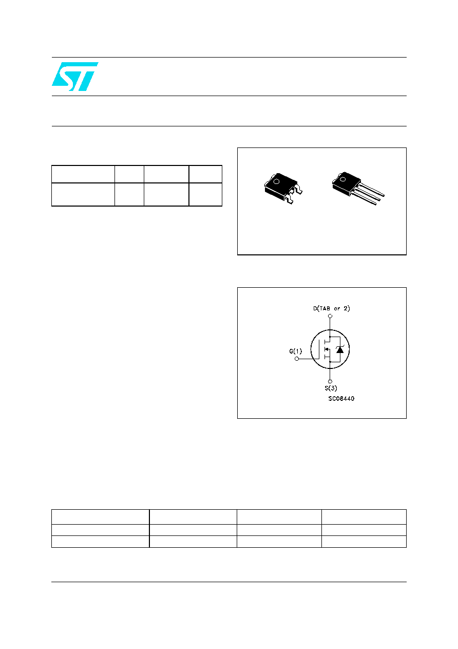
STD100NH02L
STD100NH02L-1
N-channel 24V - 0.0042
- 60A - DPAK - IPAK
STripFETTM II Power MOSFET
General features
R
DS(on)
* Qg industry's benchmark
Conduction losses reduced
Switching losses reduced
Low threshold device
Description
This device utilizes the latest advanced design
rules of ST's proprietary STripFETTM technology.
This is suitable fot the most demanding DC-DC
converter application where high efficiency is to
be achieved.
Applications
Switching application
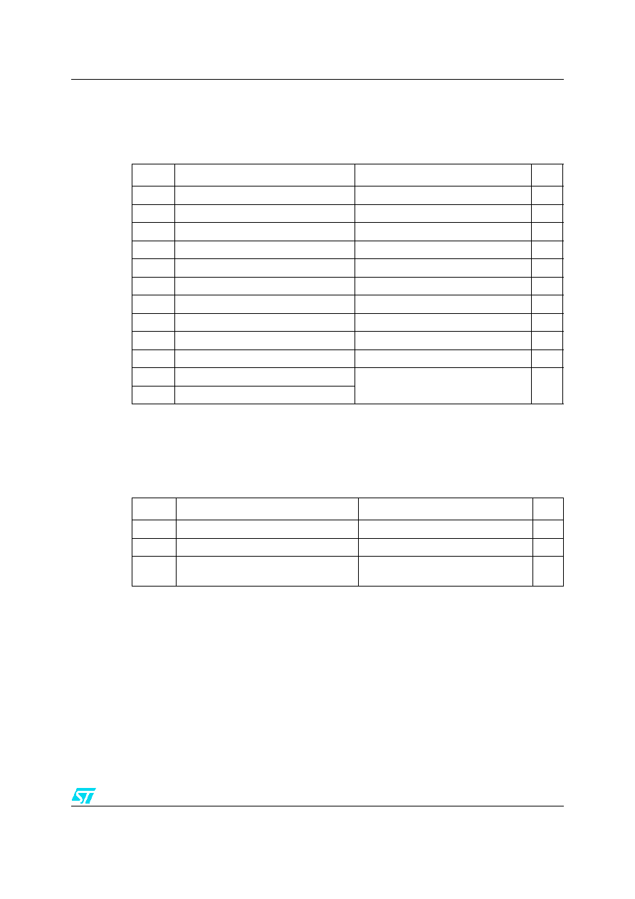
Internal schematic diagram
Type
V
DSSS
R
DS(on)
I
D
STD100NH02L
STD100NH02L-1
24V
24V
<0.0048
<0.0048
60A
(1)
60A
(1)
1.
Value limited by wire bonding
1
3
DPAK
3
2
1
IPAK
www.st.com
Order codes
Part number
Marking
Package
Packaging
STD100NH02LT4
D100NH02L
DPAK
Tape & reel
STD100NH02L-1
D100NH02L
IPAK
Tube

Contents
STD100NH02L
2/16
Contents
1
Electrical ratings . . . . . . . . . . . . . . . . . . . . . . . . . . . . . . . . . . . . . . . . . . . . 3
2
Electrical characteristics . . . . . . . . . . . . . . . . . . . . . . . . . . . . . . . . . . . . . 4
2.1
Electrical characteristics (curves) . . . . . . . . . . . . . . . . . . . . . . . . . . . . 6
3
Test circuit . . . . . . . . . . . . . . . . . . . . . . . . . . . . . . . . . . . . . . . . . . . . . . . . 8
4
Package mechanical data . . . . . . . . . . . . . . . . . . . . . . . . . . . . . . . . . . . . . 9
5
Packaging mechanical data . . . . . . . . . . . . . . . . . . . . . . . . . . . . . . . . . . 12
6
Revision history . . . . . . . . . . . . . . . . . . . . . . . . . . . . . . . . . . . . . . . . . . . 15
STD100NH02L
Electrical ratings
3/16
1 Electrical
ratings
Table 1.
Absolute maximum ratings
Symbol
Parameter
Value
Unit
V
spike
(1)
1.
Garanted when external Rg = 4.7
and t
f
< t
fmax
.
Drain-source voltage rating
30
V
V
DS
Drain-source voltage (V
GS
= 0)
24
V
V
DGR
Drain-gate voltage (R
GS
= 20K
)
24
V
V
GS
Drain-source voltage
± 20
V
I
D
(2)
2.
Value limited by wire bonding.
Drain current (continuous) at T
C
= 25°C
60
A
I
D
(2)
Drain current (continuous) at T
C
=100°C
60
A
I
DM
(3)
3.
Pulse width limited by safe operating area
Drain current (pulsed)
240
A
P
TOT
Total dissipation at T
C
= 25°C
100
W
Derating factor
0.67
W/°C
E
AS
(4)
4.
Starting T
J
= 25
o
C, I
D
= 30A, V
DD
= 15V
Single pulse avalanche energy
800
mJ
T
stg
Storage temperature
-55 to 175
°C
T
J
Max. operating junction temperature
Table 2.
Thermal data
Symbol
Parameter
Value
Unit
R
thJC
Thermal resistance junction-case Max
1.5
°C/W
R
thJA
Thermal resistance junction-ambient Max
100
°C/W
T
l
Maximum lead temperature for soldering
purpose
275
°C

Electrical characteristics
STD100NH02L
4/16
2 Electrical
characteristics
(T
CASE
=25°C unless otherwise specified)
Table 3.
On/off states
Symbol
Parameter
Test conditions
Min.
Typ.
Max.
Unit
V
(BR)DSS
Drain-source breakdown
voltage
I
D
= 25mA, V
GS
= 0
24
V
I
DSS
Zero gate voltage drain
current (V
GS
= 0)
V
DS
= 20
V
DS
= 20, T
C
= 125°C
1
10
µA
µA
I
GSS
Gate body leakage current
(V
DS
= 0)
V
GS
= ±20V
±100
nA
V
GS(th)
Gate threshold voltage
V
DS
= V
GS
, I
D
= 250µA
1
1.8
V
R
DS(on)
Static drain-source on
resistance
V
GS
= 10V, I
D
= 30A
V
GS
= 5V, I
D
= 15A
0.0042
0.005
0.0048
0.09
Table 4.
Dynamic
Symbol
Parameter
Test conditions
Min.
Typ.
Max.
Unit
g
fs
(1)
1.
Pulsed: pulse duration=300µs, duty cycle 1.5%
Forward transconductance
V
DS
= 10 V
,
I
D
= 30A
50
S
C
iss
C
oss
C
rss
Input capacitance
Output capacitance
Reverse transfer
capacitance
V
DS
= 15V, f = 1 MHz,
V
GS
= 0
3940
1020
110
pF
pF
pF
Q
g
Q
gs
Q
gd
Total gate charge
Gate-source charge
Gate-drain charge
V
DD
= 10V, I
D
= 30A
V
GS
= 10V
62
12
8
84
nC
nC
nC
Q
oss
(2)
2.
Q
oss =
C
oss
*
V
in ,
C
oss =
C
gd +
C
ds .
See
Chapter Appendix A
Output charge
V
DS
= 16V, V
GS
= 0V
24
nC
Q
gls
(3)
3.
Gate charge for synchronous operation
Third-quadrant gate charge
V
DS
< 0V, V
GS
= 10V
56.5
nC
R
G
Gate input resistance
f = 1MHz gate DC Bias = 0
Test signal level = 20mV
Open drain
1.1
STD100NH02L
Electrical characteristics
5/16
Table 5.
Switching times
Symbol
Parameter
Test conditions
Min.
Typ.
Max.
Unit
t
d(on)
t
r
t
d(off)
t
f
Turn-on delay time
Rise time
Turn-off delay time
Fall time
V
DD
= 10V, I
D
= 30A,
R
G
= 4.7
, V
GS
= 10V
Figure 13 on page 8
15
200
60
35
47
ns
ns
ns
ns
Table 6.
Source drain diode
Symbol
Parameter
Test conditions
Min
Typ.
Max
Unit
I
SD
Source-drain current
60
A
I
SDM
Source-drain current (pulsed)
240
A
V
SD
(1)
1.
Pulsed: pulse duration=300µs, duty cycle 1.5%
Forward on voltage
I
SD
= 30A, V
GS
= 0
1.3
V
t
rr
Q
rr
I
RRM
Reverse recovery time
Reverse recovery charge
Reverse recovery current
I
SD
= 60A,
di/dt = 100A/µs,
V
DD
= 15V, T
J
= 150°C
Figure 15 on page 8
47
58
2.5
ns
µC
A
Document Outline