
1/7
PRELIMINARY DATA
November 2001
This is preliminary information on a new product now in development or undergoing evaluation. Details are subject to change without notice.
STD10NF06L
N-CHANNEL 60V - 0.1
- 10A DPAK
STripFETTM POWER MOSFET
(1) I
SD
10A, di/dt
400A/µs, V
DD
=48V, T
j
T
JMAX.
(2) Starting T
j
= 25∞C, I
d
= 7A, V
DD
=20 V
s
TYPICAL R
DS
(on) = 0.1
s
SURFACE-MOUNTING DPAK (TO-252) POWER
PACKAGE IN TAPE & REEL (SUFFIX "T4")
DESCRIPTION
This MOSFET series realized with STMicroelectronics
unique STripFET
TM
process has specifically been de-
signed to minimize input capacitance and gate charge.
It is therefore suitable as primary switch in advanced
high-efficiency, high-frequency isolated DC-DC con-
verters for Telecom and Computer applications. It is
also intended for any applications with low gate drive
requirements.
APPLICATIONS
s
DC-DC & DC-AC CONVERTERS
s
DC MOTOR CONTROL
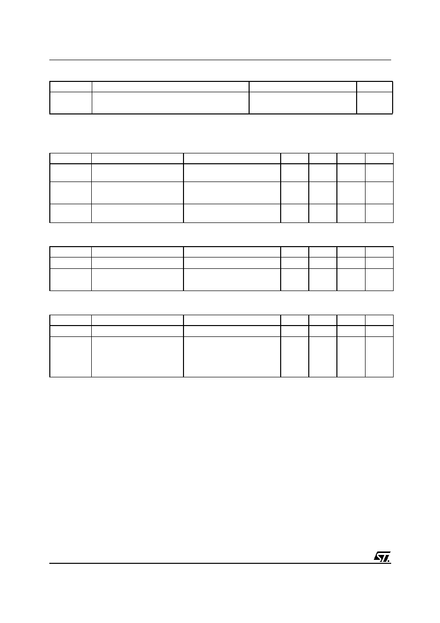
ABSOLUTE MAXIMUM RATINGS
(
q
) Pulse width limited by safe operating area
TYPE
V
DSS
R
DS(on)
I
D
STD10NF06L
60V
<0.12
10A
Symbol
Parameter
Value
Unit
V
DS
Drain-source Voltage (V
GS
= 0)
60
V
V
DGR
Drain-gate Voltage (R
GS
= 20 k
)
60
V
V
GS
Gate- source Voltage
± 15
V
I
D
Drain Current (continuos) at T
C
= 25∞C
10
A
I
D
Drain Current (continuos) at T
C
= 100∞C
7
A
I
DM
(
l
)
Drain Current (pulsed)
40
A
P
TOT
Total Dissipation at T
C
= 25∞C
30
W
Derating Factor
0.2
W/∞C
dv/dt (1)
Peak Diode Recovery voltage slope
30
V/ns
E
AS
(2)
Single Pulse Avalanche Energy
50
mJ
T
stg
Storage Temperature
≠ 55 to 175
∞C
T
j
Max. Operating Junction Temperature
DPAK
1
3
INTERNAL SCHEMATIC DIAGRAM
STD10NF06L
2/7
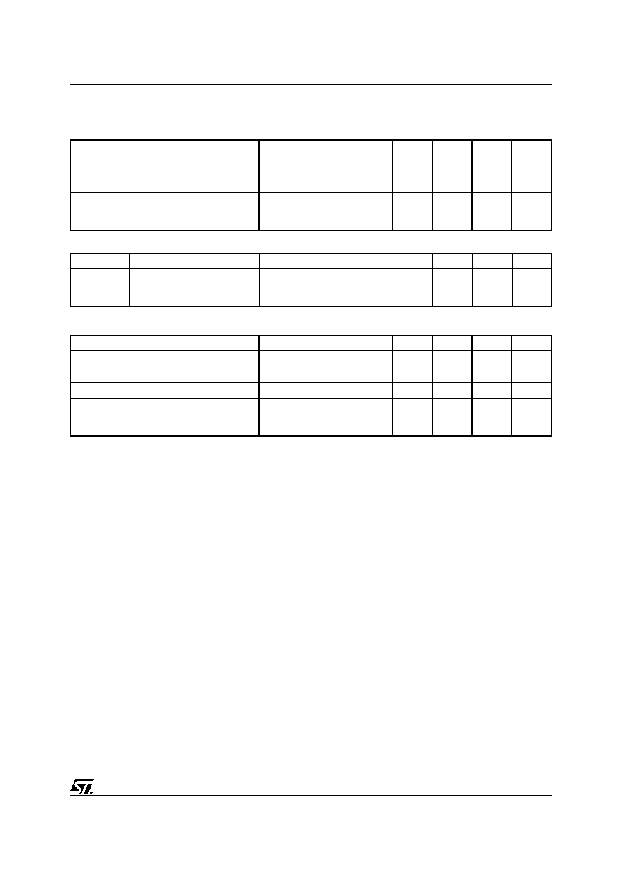
THERMAL DATA
ELECTRICAL CHARACTERISTICS (TCASE = 25 ∞C UNLESS OTHERWISE SPECIFIED)
OFF
ON
(1)
DYNAMIC
Rthj-case
Thermal Resistance Junction-case Max
5
∞C/W
Rthj-amb
Thermal Resistance Junction-ambient Max
100
∞C/W
T
l
Maximum Lead Temperature For Soldering Purpose
275
∞C
Symbol
Parameter
Test Conditions
Min.
Typ.
Max.
Unit
V
(BR)DSS
Drain-source
Breakdown Voltage
I
D
= 250 µA, V
GS
= 0
60
V
I
DSS
Zero Gate Voltage
Drain Current (V
GS
= 0)
V
DS
= Max Rating
1
µA
V
DS
= Max Rating, T
C
= 125 ∞C
10
µA
I
GSS
Gate-body Leakage
Current (V
DS
= 0)
V
GS
= ± 15V
±100
nA
Symbol
Parameter
Test Conditions
Min.
Typ.
Max.
Unit
V
GS(th)
Gate Threshold Voltage
V
DS
= V
GS
, I
D
= 250µA
1
V
R
DS(on)
Static Drain-source On
Resistance
V
GS
= 10V, I
D
= 5 A
0.1
0.12
V
GS
= 5 V, I
D
= 5 A
0.12
0.14
Symbol
Parameter
Test Conditions
Min.
Typ.
Max.
Unit
g
fs
(1)
Forward Transconductance
V
DS
=15 V
,
I
D
=10A
6
S
C
iss
Input Capacitance
V
DS
= 25V, f = 1 MHz, V
GS
= 0
346
pF
C
oss
Output Capacitance
54
pF
C
rss
Reverse Transfer
Capacitance
22
pF
3/7
STD10NF06L
ELECTRICAL CHARACTERISTICS (CONTINUED)
SWITCHING ON
SWITCHING OFF
SOURCE DRAIN DIODE
Note: 1. Pulsed: Pulse duration = 300 µs, duty cycle 1.5 %.
2. Pulse width limited by safe operating area.
Symbol
Parameter
Test Conditions
Min.
Typ.
Max.
Unit
t
d(on)
Turn-on Delay Time
V
DD
= 30V, I
D
= 5A
R
G
= 4.7
V
GS
= 4.5V
(see test circuit, Figure 3)
10
ns
t
r
Rise Time
50
ns
Q
g
Q
gs
Q
gd
Total Gate Charge
Gate-Source Charge
Gate-Drain Charge
V
DD
= 48V, I
D
= 10A,
V
GS
= 5V
6
3
2.5
8
nC
nC
nC
Symbol
Parameter
Test Conditions
Min.
Typ.
Max.
Unit
t
d(off)
t
f
Turn-off-Delay Time
Fall Time
V
DD
= 30V, I
D
= 5A,
R
G
= 4.7
,
V
GS
= 4.5V
(see test circuit, Figure 5)
20
10
ns
ns
Symbol
Parameter
Test Conditions
Min.
Typ.
Max.
Unit
I
SD
Source-drain Current
10
A
I
SDM
(2)
Source-drain Current (pulsed)
40
A
V
SD
(1)
Forward On Voltage
I
SD
= 10A, V
GS
= 0
1.3
V
t
rr
Q
rr
I
RRM
Reverse Recovery Time
Reverse Recovery Charge
Reverse Recovery Current
I
SD
= 10A, di/dt = 100A/µs,
V
DD
= 20V, T
j
= 150∞C
(see test circuit, Figure 5)
30
50
3
ns
nC
A

STD10NF06L
4/7
Fig. 5: Test Circuit For Inductive Load Switching
And Diode Recovery Times
Fig. 4: Gate Charge test Circuit
Fig. 2: Unclamped Inductive Waveform
Fig. 1: Unclamped Inductive Load Test Circuit
Fig. 3: Switching Times Test Circuit For
Resistive Load
5/7
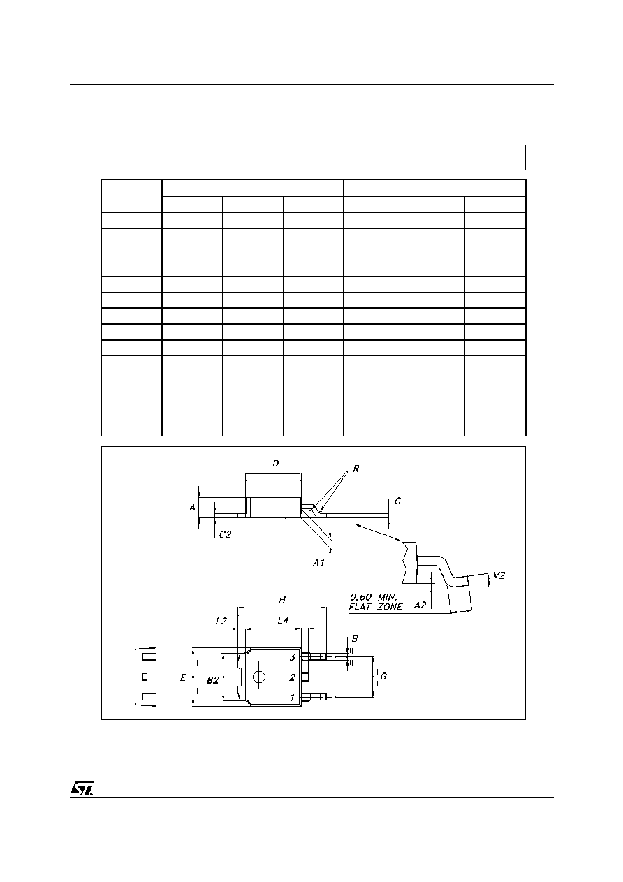
STD10NF06L
DIM.
mm
inch
MIN.
TYP.
MAX.
MIN.
TYP.
MAX.
A
2.20
2.40
0.087
0.094
A1
0.90
1.10
0.035
0.043
A2
0.03
0.23
0.001
0.009
B
0.64
0.90
0.025
0.035
B2
5.20
5.40
0.204
0.213
C
0.45
0.60
0.018
0.024
C2
0.48
0.60
0.019
0.024
D
6.00
6.20
0.236
0.244
E
6.40
6.60
0.252
0.260
G
4.40
4.60
0.173
0.181
H
9.35
10.10
0.368
0.398
L2
0.8
0.031
L4
0.60
1.00
0.024
0.039
V2
0
o
8
o
0
o
0
o
P032P_B
TO-252 (DPAK) MECHANICAL DATA