 | –≠–ª–µ–∫—Ç—Ä–æ–Ω–Ω—ã–π –∫–æ–º–ø–æ–Ω–µ–Ω—Ç: STD13003 | –°–∫–∞—á–∞—Ç—å:  PDF PDF  ZIP ZIP |
STD13003
HIGH VOLTAGE FAST-SWITCHING
NPN POWER TRANSISTOR
s
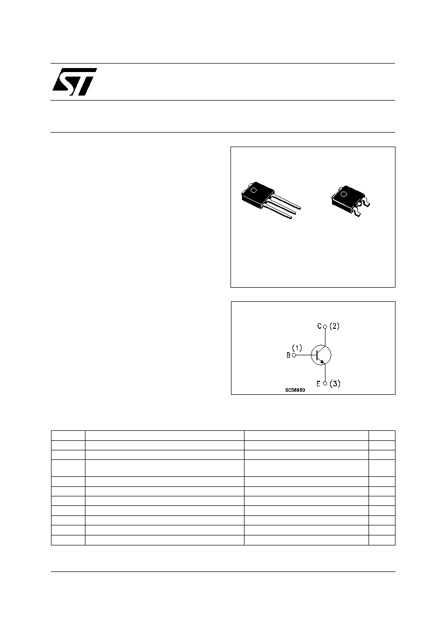
REVERSE PINS OUT Vs STANDARD IPAK
(TO-251) / DPAK (TO-252) PACKAGES
s
MEDIUM VOLTAGE CAPABILITY
s
LOW SPREAD OF DYNAMIC PARAMETERS
s
MINIMUM LOT-TO-LOT SPREAD FOR
RELIABLE OPERATION
s
VERY HIGH SWITCHING SPEED
s
SURFACE-MOUNTING DPAK (TO-252)
POWER PACKAGE IN TAPE & REEL (Suffix
"T4")
s
THROUGH-HOLE IPAK (TO-251) POWER
PACKAGE IN TUBE (Suffix "-1")
APPLICATIONS:
s
ELECTRONIC BALLASTS FOR
FLUORESCENT LIGHTING
s
SWITCH MODE POWER SUPPLIES
DESCRIPTION
The device is manufactured using high voltage
Multi Epitaxial Planar technology for high
switching speeds and medium voltage capability.
It uses a Cellular Emitter structure with planar
edge termination to enhance switching speeds
while maintaining the wide RBSOA.
The device is designed for use in lighting
applications and low cost switch-mode power
supplies.
Æ
INTERNAL SCHEMATIC DIAGRAM
September 2001
ABSOLUTE MAXIMUM RATINGS
Symbol
Parameter
Value
Unit
V
CES
Collector-Emitter Voltage (V
BE
= 0)
700
V
V
CEO
Collector-Emitter Voltage (I
B
= 0)
400
V
V
EBO
Emitter-Base Voltage
(I
C
= 0, I
B
= 0.75 A, t
p
< 10
µ
s, T
j
< 150
o
C)
BV
EBO
V
I
C
Collector Current
1.5
A
I
CM
Collector Peak Current (t
p
< 5 ms)
3
A
I
B
Base Current
0.75
A
I
BM
Base Peak Current (t
p
< 5 ms)
1.5
A
P
tot
Total Dissipation at T
c
= 25
o
C
20
W
T
stg
Storage Temperature
-65 to 150
o
C
T
j
Max. Operating Junction Temperature
150
o
C
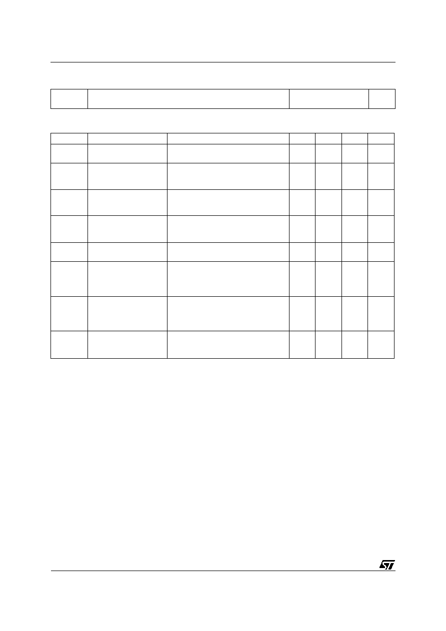
3
2
1
IPAK
TO-251
(Suffix "-1")
1
3
DPAK
TO-252
(Suffix "T4")
1/8
THERMAL DATA
R
thj-case
R
thj-amb
Thermal Resistance Junction-case Max
Thermal Resistance Junction-ambient Max
6.25
100
o
C/W
o
C/W
ELECTRICAL CHARACTERISTICS (T
case
= 25
o
C unless otherwise specified)
Symbol
Parameter
Test Conditions
Min.
Typ.
Max.
Unit
I
CEV
Collector Cut-off
Current (V
BE
= -1.5V)
V
CE
= 700V
V
CE
= 700V T
j
= 125
o
C
1
5
mA
mA
BV
EBO
Emitter-Base
Breakdown Voltage
(I
C
= 0)
I
E
= 10 mA
9
18
V
V
CEO(sus)
Collector-Emitter
Sustaining Voltage
(I
B
= 0)
I
C
= 10 mA
L = 25 mH
400
V
V
CE(sat)
Collector-Emitter
Saturation Voltage
I
C
= 0.5 A I
B
= 0.1 A
I
C
= 1 A I
B
= 0.25 A
I
C
= 1.5 A I
B
= 0.5 A
0.5
1
3
V
V
V
V
BE(sat)
Base-Emitter
Saturation Voltage
I
C
= 0.5 A I
B
= 0.1 A
I
C
= 1 A I
B
= 0.25 A
1
1.2
V
V
h
FE
DC Current Gain
I
C
= 0.5 A V
CE
= 2 V
Group A
Group B
I
C
= 1 A V
CE
= 2 V
8
15
5
20
35
25
t
r
t
s
t
f
RESISTIVE LOAD
Rise Time
Storage Time
Fall Time
I
C
= 1 A V
CC
= 125 V
I
B1
= 0.2 A I
B2
= -0.2 A
T
p
= 25
µ
s
1
4
0.7
µ
s
µ
s
µ
s
t
s
INDUCTIVE LOAD
Storage Time
I
C
= 1 A I
B1
= 0.2 A
V
BE
= -5 V L = 50 mH
V
clamp
= 300 V
0.8
µ
s
Pulsed: Pulse duration = 300
µ
s, duty cycle = 1.5 %
Note : Product is pre-selected in DC current gain (GROUP A and GROUP B). STMicroelectronics reserves the right to ship either groups
according to production availability. Please contact your nearest STMicroelectronics sales office for delivery details.
STD13003
2/8
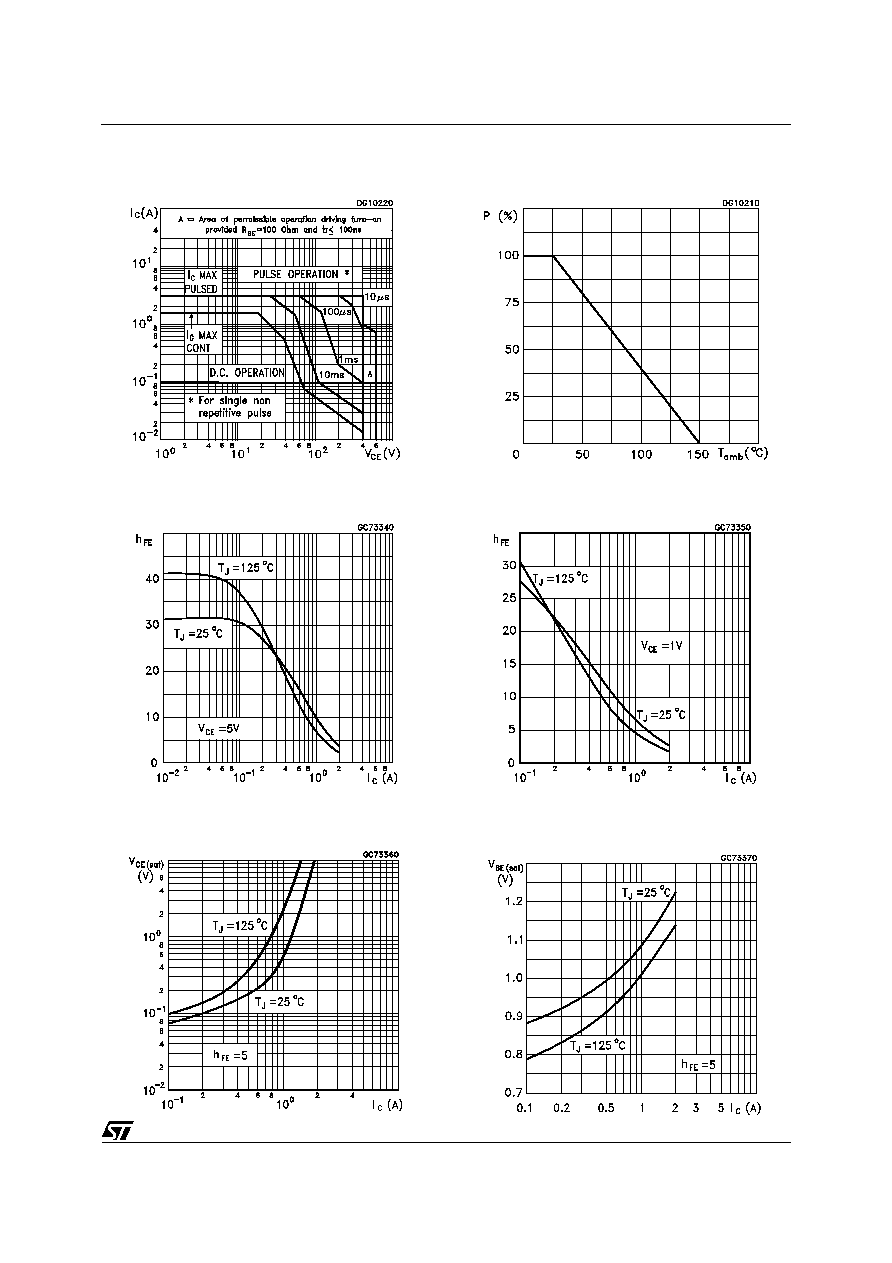
Safe Operating Areas
DC Current Gain
Collector Emitter Saturation Voltage
Derating Curve
DC Current Gain
Base Emitter Saturation Voltage
STD13003
3/8
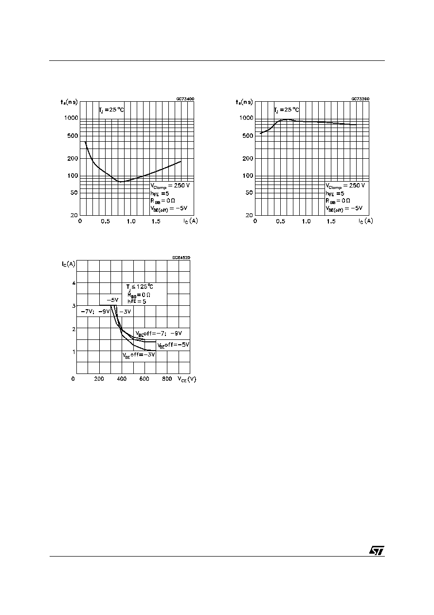
Inductive Fall Time
Inductive Storage Time
Reverse Biased SOA
STD13003
4/8
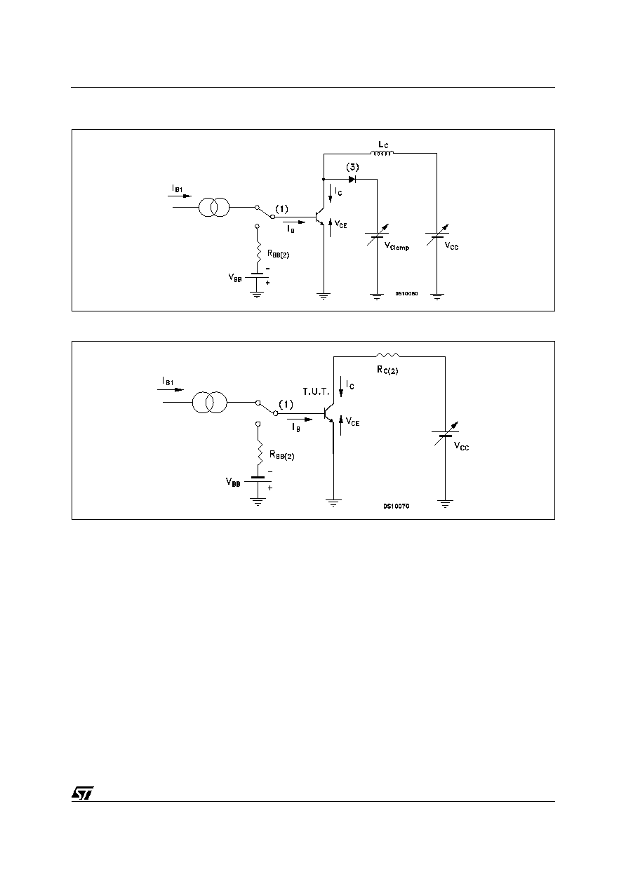
Figure 1: Inductive Load Switching Test Circuit.
Figure 2: Resistive Load Switching Test Circuit.
1) Fast electronic switch
2) Non-inductive Resistor
3) Fast recovery rectifier
1) Fast electronic switch
2) Non-inductive Resistor
STD13003
5/8
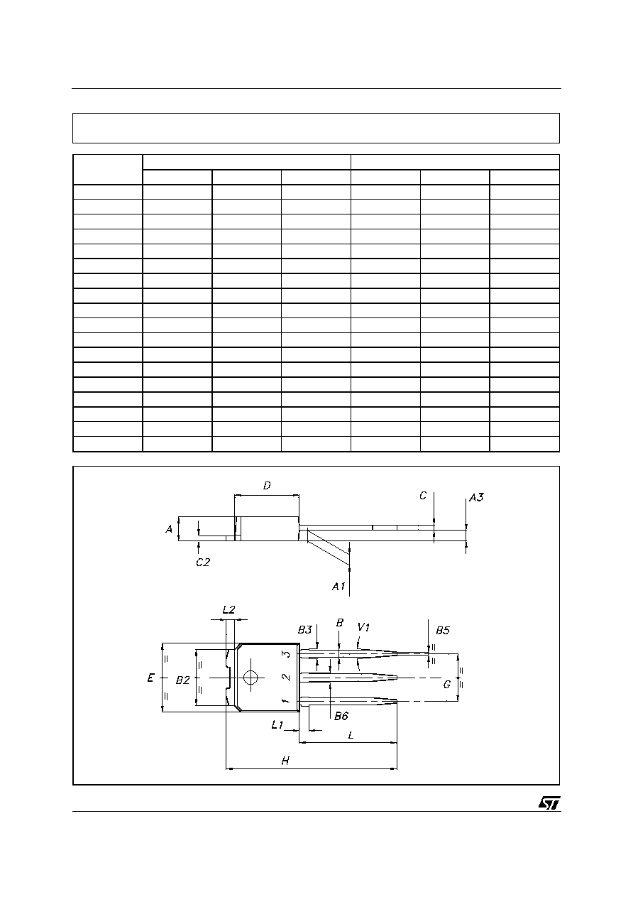
DIM.
mm
inch
MIN.
TYP.
MAX.
MIN.
TYP.
MAX.
A
2.20
2.40
0.087
0.094
A1
0.90
1.10
0.035
0.043
A3
0.70
1.30
0.028
0.051
B
0.64
0.90
0.025
0.035
B2
5.20
5.40
0.204
0.213
B3
0.85
0.033
B5
0.30
0.012
B6
0.95
0.037
C
0.45
0.60
0.018
0.024
C2
0.48
0.60
0.019
0.024
D
6.00
6.20
0.237
0.244
E
6.40
6.60
0.252
0.260
G
4.40
4.60
0.173
0.181
H
15.90
16.30
0.626
0.642
L
9.00
9.40
0.354
0.370
L1
0.80
1.20
0.031
0.047
L2
0.80
1.00
0.031
0.039
V1
10
o
10
o
P032N_E
TO-251 (IPAK) MECHANICAL DATA
STD13003
6/8
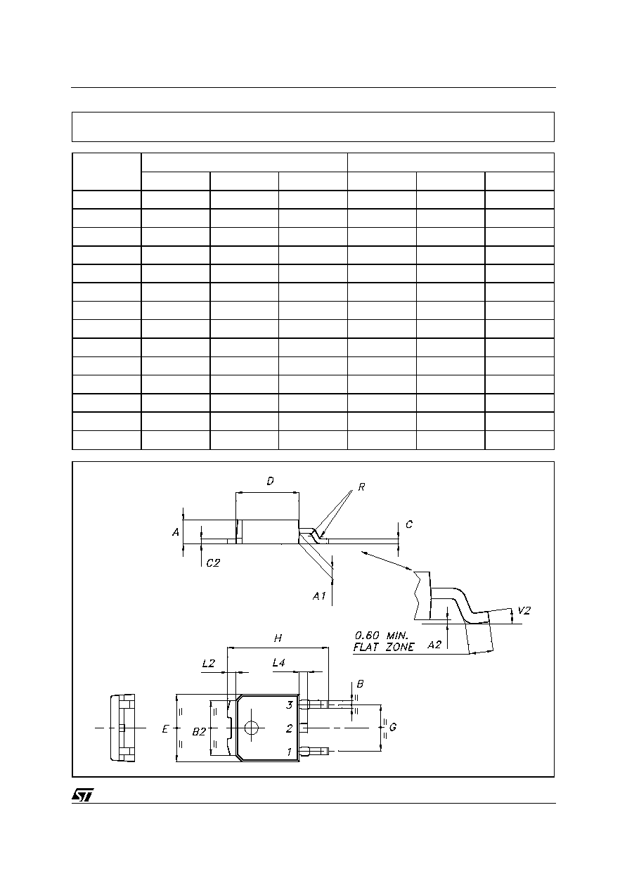
DIM.
mm
inch
MIN.
TYP.
MAX.
MIN.
TYP.
MAX.
A
2.20
2.40
0.087
0.094
A1
0.90
1.10
0.035
0.043
A2
0.03
0.23
0.001
0.009
B
0.64
0.90
0.025
0.035
B2
5.20
5.40
0.204
0.213
C
0.45
0.60
0.018
0.024
C2
0.48
0.60
0.019
0.024
D
6.00
6.20
0.236
0.244
E
6.40
6.60
0.252
0.260
G
4.40
4.60
0.173
0.181
H
9.35
10.10
0.368
0.398
L2
0.8
0.031
L4
0.60
1.00
0.024
0.039
V2
0
o
8
o
0
o
0
o
P032P_B
TO-252 (DPAK) MECHANICAL DATA
STD13003
7/8

Information furnished is believed to be accurate and reliable. However, STMicroelectronics assumes no responsibility for the consequences
of use of such information nor for any infringement of patents or other rights of third parties which may result from its use. No license is
granted by implication or otherwise under any patent or patent rights of STMicroelectronics. Specification mentioned in this publication are
subject to change without notice. This publication supersedes and replaces all information previously supplied. STMicroelectronics products
are not authorized for use as critical components in life support devices or systems without express written approval of STMicroelectronics.
The ST logo is a trademark of STMicroelectronics
© 2001 STMicroelectronics ≠ Printed in Italy ≠ All Rights Reserved
STMicroelectronics GROUP OF COMPANIES
Australia - Brazil - China - Finland - France - Germany - Hong Kong - India - Italy - Japan - Malaysia - Malta - Morocco -
Singapore - Spain - Sweden - Switzerland - United Kingdom - U.S.A.
http://www.st.com
STD13003
8/8