Äîêóìåíòàöèÿ è îïèñàíèÿ www.docs.chipfind.ru
1/9
PRELIMINARY DATA
September 2003
This is preliminary information on a new product now in development or undergoing evaluation. Details are subject to change without notice.
STD150NH02L
N-CHANNEL 24V - 0.003
- 150A ClipPAKTM/IPAK
STripFETTM III POWER MOSFET
s
TYPICAL R
DS
(on) = 0.003
@ 10 V
s
TYPICAL R
DS
(on) = 0.005
@ 5 V
s
R
DS(ON)
* Qg INDUSTRY's BENCHMARK
s
CONDUCTION LOSSES REDUCED
s
SWITCHING LOSSES REDUCED
s
LOW THRESHOLD DEVICE
s
THROUGH-HOLE IPAK (TO-251) POWER
PACKAGE IN TUBE (SUFFIX "-1")
s
SURFACE-MOUNTING POWER PACKAGE
IN TAPE & REEL (SUFFIX "T4")
DESCRIPTION
The STD150NH02L utilizes the latest advanced design
rules of ST's proprietary STripFETTM technology. This
novel 0.6
µ
process utilizes also unique metallization
techniques that couple to a "bondless" assembly
technique result in outstanding performance with
standard DPAK outline. It is therefore ideal in high
performance DC-DC converter applications where
efficiency it to be achieved at very high out currents.
APPLICATIONS
s
SPECIFICALLY DESIGNED AND OPTIMISED
FOR HIGH EFFICIENCY DC/DC CONVERTES
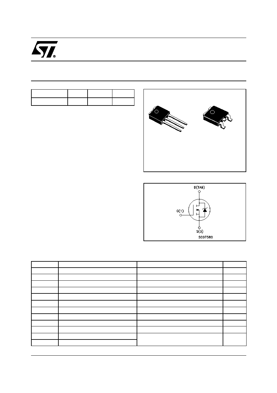
TYPE
V
DSS
R
DS(on)
I
D
STD150NH02L
24 V
< 0.0035
150 A
ClipPakTM
(Suffix "T4")
3
2
1
1
3
IPAK
TO-251
(Suffix "-1")
ABSOLUTE MAXIMUM RATINGS
Symbol
Parameter
Value
Unit
V
spike(1)
Drain-source Voltage Rating
30
V
V
DS
Drain-source Voltage (V
GS
= 0)
24
V
V
DGR
Drain-gate Voltage (R
GS
= 20 k
)
24
V
V
GS
Gate- source Voltage
± 20
V
I
D
Drain Current (continuous) at T
C
= 25°C
150
A
I
D
Drain Current (continuous) at T
C
= 100°C
95
A
I
DM(2)
Drain Current (pulsed)
600
A
P
tot
Total Dissipation at T
C
= 25°C
125
W
Derating Factor
0.83
W/°C
E
AS (3)
Single Pulse Avalanche Energy
900
mJ
T
stg
Storage Temperature
-55 to 175
°C
T
j
Max. Operating Junction Temperature
INTERNAL SCHEMATIC DIAGRAM
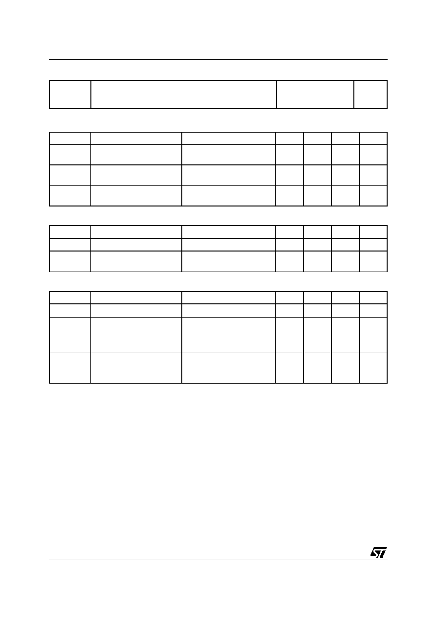
STD150NH02L
2/9
THERMAL DATA
ELECTRICAL CHARACTERISTICS (T
CASE
= 25 °C UNLESS OTHERWISE SPECIFIED)
OFF
ON
(4)
DYNAMIC
Rthj-case
Rthj-amb
T
l
Thermal Resistance Junction-case
Thermal Resistance Junction-ambient
Maximum Lead Temperature For Soldering Purpose
Max
Max
1.2
100
275
°C/W
°C/W
°C
Symbol
Parameter
Test Conditions
Min.
Typ.
Max.
Unit
V
(BR)DSS
Drain-source
Breakdown Voltage
I
D
= 25 mA, V
GS
= 0
24
V
I
DSS
Zero Gate Voltage
Drain Current (V
GS
= 0)
V
DS
= 20 V
V
DS
= 20 V T
C
= 125°C
1
10
µA
µA
I
GSS
Gate-body Leakage
Current (V
DS
= 0)
V
GS
= ± 20V
±100
nA
Symbol
Parameter
Test Conditions
Min.
Typ.
Max.
Unit
V
GS(th)
Gate Threshold Voltage
V
DS
= V
GS
I
D
= 250 µA
1
1.8
V
R
DS(on)
Static Drain-source On
Resistance
V
GS
= 10 V
I
D
= 75 A
V
GS
= 5 V
I
D
= 75 A
0.003
0.005
0.0035
0.0065
Symbol
Parameter
Test Conditions
Min.
Typ.
Max.
Unit
g
fs (4)
Forward Transconductance
V
DS
= 10 V
I
D
= 40 A
52
S
C
iss
C
oss
C
rss
Input Capacitance
Output Capacitance
Reverse Transfer
Capacitance
V
DS
= 15V f = 1 MHz V
GS
= 0
4450
1126
141
pF
pF
pF
R
G
Gate Input Resistance
f = 1 MHz Gate DC Bias = 0
Test Signal Level = 20 mV
Open Drain
1.6
3/9
STD150NH02L
SWITCHING ON
SWITCHING OFF
SOURCE DRAIN DIODE
(1)
Garanted when external Rg=4.7
and t
f
< t
fmax
.
(4)
Pulsed: Pulse duration = 300 µs, duty cycle 1.5 %.
(2)
Pulse width limited by safe operating area
(5)
Q
oss =
C
oss
*
V
in ,
C
oss =
C
gd +
C
ds .
See Appendix A
(
3
) Starting T
j
= 25
o
C, I
D
= 150A, V
DD
= 10V
(6)
Gate charge for synchronous operation
.
.
Symbol
Parameter
Test Conditions
Min.
Typ.
Max.
Unit
t
d(on)
t
r
Turn-on Delay Time
Rise Time
V
DD
= 10 V
I
D
= 75 A
R
G
= 4.7
V
GS
= 10 V
(Resistive Load, Figure 3)
14
224
ns
ns
Q
g
Q
gs
Q
gd
Total Gate Charge
Gate-Source Charge
Gate-Drain Charge
V
DD
= 16V I
D
= 150A V
GS
= 10 V
69
13
9
93
nC
nC
nC
Q
oss(5)
Output Charge
V
DS
= 16 V V
GS
= 0 V
27
nC
Q
gls(6)
Third-quadrant Gate Charge
V
DS
< 0 V V
GS
= 10 V
64
nC
Symbol
Parameter
Test Conditions
Min.
Typ.
Max.
Unit
t
d(off)
t
f
Turn-off Delay Time
Fall Time
V
DD
= 10 V
I
D
= 75 A
R
G
= 4.7
,
V
GS
= 10 V
(Resistive Load, Figure 3)
69
40
54
ns
ns
Symbol
Parameter
Test Conditions
Min.
Typ.
Max.
Unit
I
SD
I
SDM
Source-drain Current
Source-drain Current (pulsed)
150
600
A
A
V
SD
(4)
Forward On Voltage
I
SD
= 75 A V
GS
= 0
1.3
V
t
rr
Q
rr
I
RRM
Reverse Recovery Time
Reverse Recovery Charge
Reverse Recovery Current
I
SD
= 150 A
di/dt = 100A/µs
V
DD
= 15 V
T
j
= 150°C
(see test circuit, Figure 5)
47
58
2.5
ns
nC
A
ELECTRICAL CHARACTERISTICS (continued)
STD150NH02L
4/9
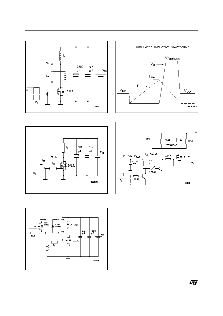
Fig. 1: Unclamped Inductive Load Test Circuit
Fig. 1: Unclamped Inductive Load Test Circuit
Fig. 2: Unclamped Inductive Waveform
Fig. 3: Switching Times Test Circuits For Resistive
Load
Fig. 4: Gate Charge test Circuit
Fig. 5: Test Circuit For Inductive Load Switching
And Diode Recovery Times
5/9
STD150NH02L
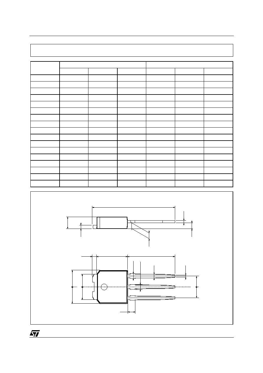
DIM.
mm
inch
MIN.
TYP.
MAX.
MIN.
TYP.
MAX.
A
2.2
2.4
0.086
0.094
A1
0.9
1.1
0.035
0.043
A3
0.7
1.3 0.027
0.051
B
0.64
0.9
0.025
0.031
B2
5.2
5.4
0.204
0.212
B3
0.85
0.033
B5
0.3
0.012
B6
0.95
0.037
C
0.45
0.6
0.017
0.023
C2
0.48
0.6
0.019
0.023
D
6
6.2
0.236
0.244
E
6.4
6.6
0.252
0.260
G
4.4
4.6
0.173
0.181
H
15.9
16.3
0.626
0.641
L
9
9.4
0.354
0.370
L1
0.8
1.2
0.031
0.047
L2
0.8
1
0.031
0.039
A
C2
C
A3
H
A1
D
L
L2
L1
1 3
= =
B3
B
B6
B2
E
G
= =
= =
B5
2
TO-251 (IPAK) MECHANICAL DATA
0068771-E

STD150NH02L
6/9
DIM.
mm
inch
MIN.
TYP.
MAX.
MIN.
TYP.
MAX.
A
2.2
2.4
0.086
0.094
A1
0.9
1.1
0.035
0.043
A2
0.03
0.23 0.001
0.009
B
0.64
0.9
0.025
0.035
B2
5.2
5.4
0.204
0.212
C
0.45
0.6
0.017
0.023
C2
0.48
0.6
0.019
0.023
D
6
6.2
0.236
0.244
E
6.4
6.6
0.252
0.260
G
4.4
4.6
0.173
0.181
H
9.35
10.1
0.368
0.397
L2
0.8
0.031
L4
0.6
1
0.023
0.039
==
D
L2
L4
1 3
==
B
E
==
B2
G
2
A
C2
C
H
A1
DETAIL "A"
A2
DETAIL "A"
TO-252 (DPAK) MECHANICAL DATA
0068772-B

7/9
STD150NH02L
SW1
SW2
APPENDIX A
Buck Converter: Power Losses Estimation
The power losses associated with the FETs in a Synchronous Buck converter can be
estimated using the equations shown in the table below. The formulas give a good
approximation, for the sake of performan
ce comparison, of how different pairs of devices
affect the converter efficiency. However a very important parameter, the working
temperature, is not considered. The real device behavior is really dependent on how the
heat generated inside the devices is r
emoved to allow for a safer working junction
temperature.
The low side (
SW2
) device requires:
·
Very low R
DS(on)
to reduce conduction losses
·
Small Q
gls
to reduce the gate charge losses
·
Small C
oss
to reduce losses due to output capacitance
·
Small Q
rr
to reduce losses on SW
1
during its turn-on
·
The C
gd
/C
gs
ratio lower than V
th
/V
gg
ratio especially with low drain to source
voltage to avoid the cross conduction phenomenon;
The high side (
SW1)
device requires:
·
Small R
g
and L
s
to allow higher gate current peak an
d to limit the voltage
feedback on the gate
·
Small Q
g
to have a faster commutation and to reduce gate charge losses
·
Low R
DS(on)
to reduce the conduction losses.
STD150NH02L
8/9
High Side Switch (SW1)
Low Side Switch (SW2)
conduction
P
d
*
I
*
R
2
L
DS(on)SW1
)
1
(
*
I
*
R
2
L
DS(on)SW2
d
-
switching
P
g
L
I
I
*
f
*
)
Q
(Q
*
V
gd(SW1)
gsth(SW1)
in
+
Zero Voltage Switching
Recovery
Not Applicable
1
f
*
Q
*
V
rr(SW2)
in
diode
P
Conduction Not
Applicable
f
*
t
*
I
*
V
deadtime
L
f(SW2)
)
gate(Q
G
P
f
*
V
*
Q
gg
g(SW1)
f
*
V
*
Q
gg
gls(SW2)
Qoss
P
2
f
*
Q
*
V
oss(SW1)
in
2
f
*
Q
*
V
oss(SW2)
in
Parameter Meaning
d
Duty-cycle
Q
gsth
Post threshold gate charge
Q
gls
Third quadrant gate charge
Pconduction
On state losses
Pswitching
On-off transition losses
Pdiode
Conduction and reverse recovery diode losses
Pgate
Gate drive losses
Qoss
P
Output capacitance losses
1
Dissipated by SW1 during turn-on

9/9
STD150NH02L
Information furnished is believed to be accurate and reliable. However, STMicroelectronics assumes no responsibility for the consequences
of use of such information nor for any infringement of patents or other rights of third parties which may result from its use. No license is granted
by implication or otherwise under any patent or patent rights of STMicroelectronics. Specifications mentioned in this publication are subject
to change without notice. This publication supersedes and replaces all information previously supplied. STMicroelectronics products are not
authorized for use as critical components in life support devices or systems without express written approval of STMicroelectronics.
The ST logo is registered trademark of STMicroelectronics
®
2002 STMicroelectronics - All Rights Reserved
All other names are the property of their respective owners.
STMicroelectronics GROUP OF COMPANIES
Australia - Brazil - Canada - China - Finland - France - Germany - Hong Kong - India - Israel - Italy - Japan - Malaysia - Malta - Morocco -
Singapore - Spain - Sweden - Switzerland - United Kingdom - United States.
http://www.st.com