
July 2006
Rev 4
1/14
14
STD16NF06L
STD16NF06L-1
N-channel 60V - 0.060
- 24A - DPAK/IPAK
STripFETTM II Power MOSFET
General features
Logic level device
Low threshold drive
Description
This Power MOSFET is the latest development of
STMicroelectronis unique "Single Feature SizeTM"
strip-based process. The resulting transistor
shows extremely high packing density for low on-
resistance, rugged avalanche characteristics and
less critical alignment steps therefore a
remarkable manufacturing reproducibility.
Applications
Switching application
Internal schematic diagram
Type
V
DSS
R
DS(on)
I
D
STD16NF06L-1
60V
<0.070
24A
STD16NF06L
60V
<0.070
24A
DPAK
3
2
1
1
3
iPAK
www.st.com
Order codes
Part number
Marking
Package
Packaging
STD16NF06L-1
D16NF06L
IPAK
Tube
STD16NF06LT4
D16NF06L
DPAK
Tape & reel

Contents
STD16NF06L - STD16NF06L-1
2/14
Contents
1
Electrical ratings . . . . . . . . . . . . . . . . . . . . . . . . . . . . . . . . . . . . . . . . . . . . 3
2
Electrical characteristics . . . . . . . . . . . . . . . . . . . . . . . . . . . . . . . . . . . . . 4
2.1
Electrical characteristics (curves) . . . . . . . . . . . . . . . . . . . . . . . . . . . . . 6
3
Test circuit . . . . . . . . . . . . . . . . . . . . . . . . . . . . . . . . . . . . . . . . . . . . . . . . 8
4
Package mechanical data . . . . . . . . . . . . . . . . . . . . . . . . . . . . . . . . . . . . . 9
5
Packing mechanical data . . . . . . . . . . . . . . . . . . . . . . . . . . . . . . . . . . . . 12
6
Revision history . . . . . . . . . . . . . . . . . . . . . . . . . . . . . . . . . . . . . . . . . . . 13

STD16NF06L - STD16NF06L-1
Electrical ratings
3/14
1 Electrical
ratings
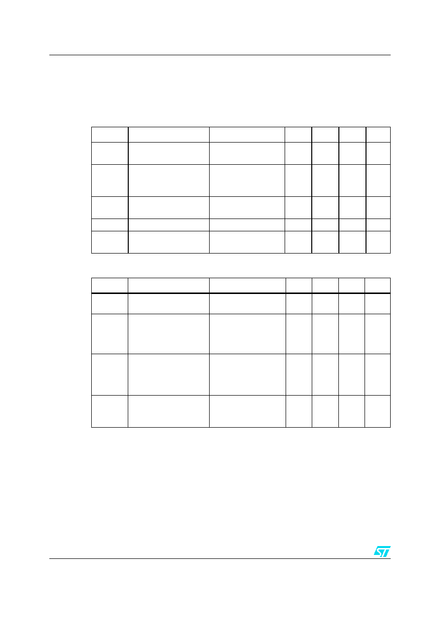
Table 1.
Absolute maximum ratings
Symbol
Parameter
Value
Unit
V
DS
Drain-source voltage (V
GS
= 0)
60
V
V
DGR
Drain-gate voltage (R
GS
= 20 k
)
60
V
V
GS
Gate- source voltage
± 18
V
I
D
Drain current (continuous) at T
C
= 25∞C
24
A
I
D
Drain current (continuous) at T
C
= 100∞C
17
A
I
DM
(1)
1.
Pulse width limited by safe operating area.
Drain current (pulsed)
96
A
P
tot
Total dissipation at T
C
= 25∞C
40
W
Derating Factor
0.27
W/∞C
dv/dt
(2)
2.
I
SD
16A, di/dt 200A/µs, V
DD
=V(
BR)DSS
, T
j
T
JMAX
Peak diode recovery avalanche energy
11.5
V/ns
E
AS
(3)
3.
Starting T
j
= 25 ∞C, I
D
= 20A, V
DD
= 48V
Single pulse avalanche energy
200
mJ
T
stg
Storage temperature
-55 to 175
∞C
T
j
Max. operating junction temperature
Table 2.
Thermal data
Rthj-case
Thermal resistance junction-case max
3.75
∞C/W
Rthj-pcb
Thermal resistance junction-to PCB max
62
∞C/W
T
J
Maximum lead temperature for soldering purpose
(1)
1.
When Mounted on 1 inch2 FR-4 board, 2 oz of Cu
300
∞C
Electrical characteristics
STD16NF06L - STD16NF06L-1
4/14
2 Electrical
characteristics
(T
CASE
=25∞C unless otherwise specified)
Table 3.
On/off states
Symbol
Parameter
Test conditions
Min.
Typ.
Max.
Unit
V
(BR)DSS
Drain-source
breakdown voltage
I
D
= 250µA, V
GS
=0
60
V
I
DSS
Zero gate voltage
drain current (V
GS
= 0)
V
DS
= Max rating
V
DS
= Max rating,
T
C
= 125∞C
1
10
µA
µA
I
GSS
Gate-body leakage
current (V
DS
= 0)
V
GS
= ± 18V
±100
nA
V
GS(th)
Gate threshold voltage
V
DS
= V
GS
, I
D
= 250µA
1
V
R
DS(on)
Static drain-source on
resistance
V
GS
= 10V, I
D
= 8A
V
GS
= 5V, I
D
= 8A
0.060
0.070
0.070
0.085
Table 4.
Dynamic
Symbol
Parameter
Test conditions
Min.
Typ.
Max.
Unit
g
fs
(1)
1.
Pulsed: Pulse duration = 300 µs, duty cycle 1.5 %.
Forward
transconductance
V
DS
= 15V
,
I
D
= 12A
12
S
C
iss
C
oss
C
rss
Input capacitance
Output capacitance
Reverse transfer
capacitance
V
DS
= 25V, f = 1MHz,
V
GS
= 0
370
69
30
pF
pF
pF
t
d(on)
t
r
t
d(off)
t
f
Turn-on delay time
Rise time
Turn-off delay time
Fall time
V
DD
= 30V, I
D
= 8A
R
G
= 4.7
V
GS
= 5V
(see
Figure 13
)
12
30
20
6
ns
ns
ns
ns
Q
g
Q
gs
Q
gd
Total gate charge
Gate-source charge
Gate-drain charge
V
DD
= 30V, I
D
= 8A,
V
GS
= 5V, R
G
= 4.7
(see
Figure 14
)
7.5
2.5
4.2
nC
nC
nC

STD16NF06L - STD16NF06L-1
Electrical characteristics
5/14
Table 5.
Source drain diode
Symbol
Parameter
Test conditions
Min.
Typ.
Max.
Unit
I
SD
I
SDM
(1)
1.
Pulse width limited by safe operating area.
Source-drain current
Source-drain current
(pulsed)
16
64
A
A
V
SD
(2)
2.
Pulsed: Pulse duration = 300 µs, duty cycle 1.5 %
Forward on voltage
I
SD
= 16A, V
GS
= 0
1.5
V
t
rr
Q
rr
I
RRM
Reverse recovery time
Reverse recovery charge
Reverse recovery current
I
SD
= 16A, di/dt = 100A/µs,
V
DD
= 25V, T
j
= 150∞C
(see
Figure 15
)
53
85
3.2
ns
µC
A