 | –≠–ª–µ–∫—Ç—Ä–æ–Ω–Ω—ã–π –∫–æ–º–ø–æ–Ω–µ–Ω—Ç: STD20N06 | –°–∫–∞—á–∞—Ç—å:  PDF PDF  ZIP ZIP |
STD20N06
N - CHANNEL ENHANCEMENT MODE
"ULTRA HIGH DENSITY" POWER MOS TRANSISTOR
PRELIMINARY DATA
s
TYPICAL R
DS(on)
= 0.026
s
AVALANCHE RUGGED TECHNOLOGY
s
100% AVALANCHE TESTED
s
REPETITIVE AVALANCHE DATA AT 100
o
C
s
HIGH CURRENT CAPABILITY
s
175
o
C OPERATING TEMPERATURE
s
HIGH dV/dt RUGGEDNESS
s
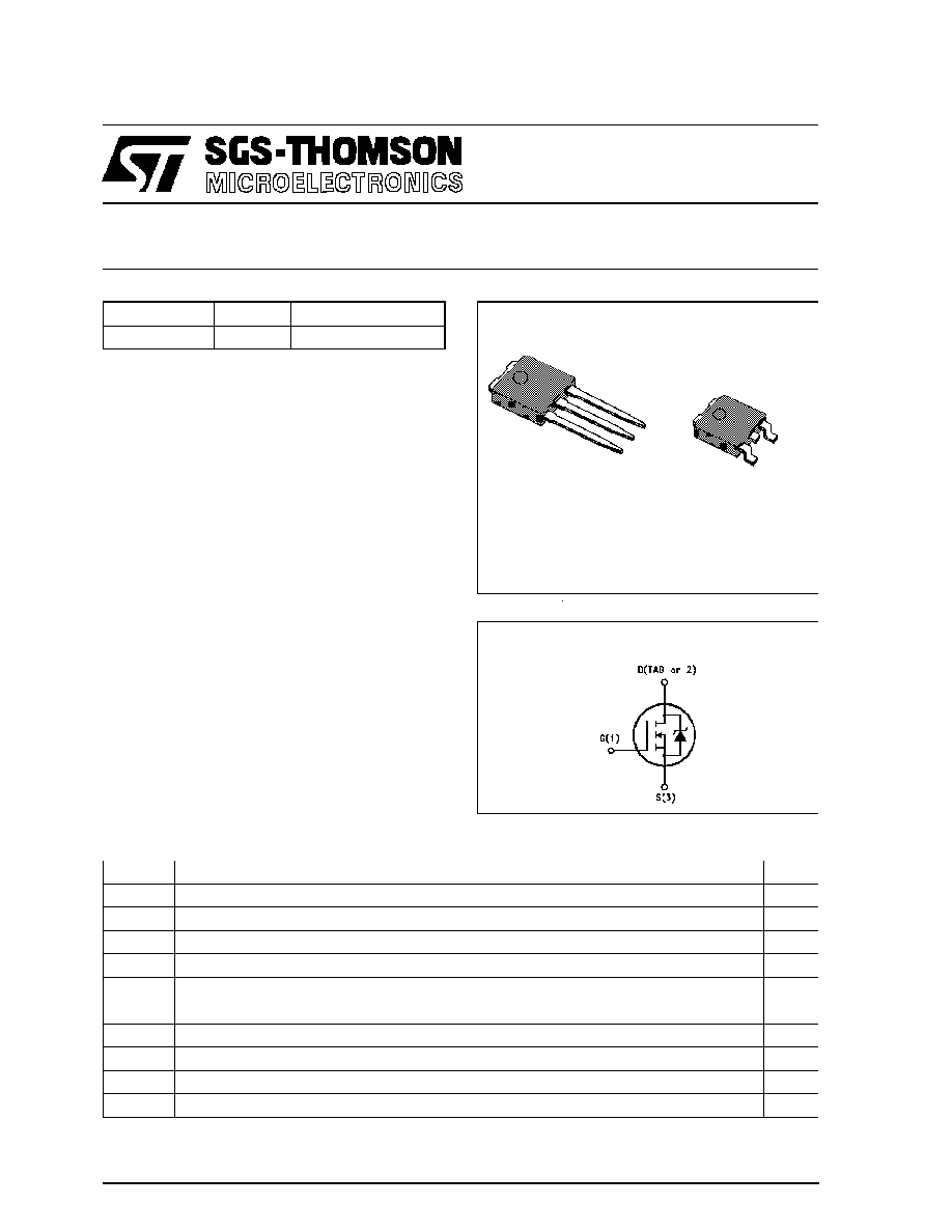
THROUGH-HOLE IPAK (TO-251) POWER
PACKAGE IN TUBE (SUFFIX "-1")
s
SURFACE-MOUNTING DPAK (TO-252)
POWER PACKAGE IN TAPE & REEL
(SUFFIX "T4")
DESCRIPTION
This series of POWER MOSFETS represents the
latest development in low voltage technology.
The ultra high cell density process (UHD) produ-
ced with fine geometries on advanced equipment
gives the device extremely low R
DS(on)
as well as
good switching performance and high avalanche
energy capability.
APPLICATIONS
s
HIGH CURRENT, HIGH SPEED SWITCHING
s
POWER MOTOR CONTROL
s
DC-DC & DC-AC CONVERTERS
s
SYNCRONOUS RECTIFICATION
INTERNAL SCHEMATIC DIAGRAM
TYPE
V
DSS
R
DS ( on)
I
D
STD20N06
60 V
< 0. 03
20 A (*)
March 1995
ABSOLUTE MAXIMUM RATINGS
Symbol
Parameter
Value
Uni t
V
D S
Drain-source Voltage (V
GS
= 0)
60
V
V
DG R
Drain- gate Voltage (R
GS
= 20 k
)
60
V
V
GS
Gate-source Voltage
±
20
V
I
D
Drain Current (cont inuous) at T
c
= 25
o
C
20
A
I
D
Drain Current (cont inuous) at T
c
= 100
o
C
14
A
I
D M
(
∑
)
Drain Current (pulsed)
80
A
P
tot
Total Dissipation at T
c
= 25
o
C
60
W
Derating Factor
0.4
W/
o
C
T
stg
St orage Temperat ure
-65 to 175
o
C
T
j
Max. Operat ing Junction Temperature
175
o
C
(*) Current limited by the package
(
∑
) Pulse width limited by safe operating area (*)
1
3
2
IPAK
TO-251
(Suffix "-1")
1
3
DPAK
TO-252
(Suffix "T4")
1/10

THERMAL DATA
R
thj-cas e
R
thj- amb
R
thj- amb
T
l
Thermal Resist ance Junct ion-case
Max
Thermal Resist ance Junct ion-ambient
Max
Thermal Resist ance Case-sink
Typ
Maximum Lead Temperature For Soldering Purpose
2.5
100
1.5
300
o
C/ W
o
C/ W
o
C/ W
o
C
AVALANCHE CHARACTERISTICS
Symbol
Parameter
Max Value
Uni t
I
A R
Avalanche Current, Repetitive or Not-Repetitive
(pulse width limited by T
j
max,
< 1%)
20
A
E
AS
Single Pulse Avalanche Energy
(st arting T
j
= 25
o
C, I
D
= I
AR
, L = 330
µ
H, V
DD
= 25 V)
(see waveforms, figure 2)
80
mJ
E
AR
Repet itive Avalanche Energy
(pulse width limited by T
j
max,
< 1%)
20
mJ
I
A R
Avalanche Current, Repetitive or Not-Repetitive
(T
c
= 100
o
C, pulse width limited by T
j
max,
< 1%)
14
A
ELECTRICAL CHARACTERISTICS (T
case
= 25
o
C unless otherwise specified)
OFF
Symbol
Parameter
Test Condi tions
Mi n.
Typ.
Max.
Unit
V
( BR)DSS
Drain-source
Breakdown Voltage
I
D
= 250
µ
A
V
G S
= 0
60
V
I
DS S
Zero Gate Volt age
Drain Current (V
GS
= 0)
V
DS
= Max Rating
V
DS
= Max Rating x 0.8
T
c
= 125
o
C
250
1000
µ
A
µ
A
I
G SS
Gate-body Leakage
Current (V
D S
= 0)
V
GS
=
±
20 V
±
100
nA
ON (
)
Symbol
Parameter
Test Condi tions
Mi n.
Typ.
Max.
Unit
V
G S(th)
Gate Threshold Voltage V
DS
= V
GS
I
D
= 250
µ
A
2
3
4
V
R
DS( on)
St atic Drain-source On
Resist ance
V
GS
= 10V
I
D
= 10 A
V
GS
= 10V
I
D
= 10 A
T
c
= 100
o
C
0. 026
0. 03
0. 06
I
D( on)
On St ate Drain Current
V
DS
> I
D( on)
x R
D S(on) max
V
GS
= 10 V
20
A
DYNAMIC
Symbol
Parameter
Test Condi tions
Mi n.
Typ.
Max.
Unit
g
fs
(
)
Forward
Transconductance
V
DS
> I
D( on)
x R
D S(on) max
I
D
= 10 A
11
16
S
C
iss
C
oss
C
rss
I nput Capacitance
Output Capacit ance
Reverse Transfer
Capacitance
V
DS
= 25 V
f = 1 MHz
V
G S
= 0
2000
350
80
2800
450
120
pF
pF
pF
STD20N06
2/10
ELECTRICAL CHARACTERISTICS (continued)
SWITCHING ON
Symbol
Parameter
Test Condi tions
Mi n.
Typ.
Max.
Unit
t
d(on)
t
r
Turn-on Time
Rise Time
V
DD
= 30 V
I
D
= 10 A
R
G
= 50
V
GS
= 10 V
(see test circuit, figure 3)
45
280
65
380
ns
ns
(di/dt)
on
Turn-on Current Slope
V
DD
= 48 V
I
D
= 20 A
R
G
= 50
V
GS
= 10 V
(see test circuit, figure 5)
240
A/
µ
s
Q
g
Q
gs
Q
gd
Total Gate Charge
Gate-Source Charge
Gate-Drain Charge
V
DD
= 40 V
I
D
= 20 A
V
GS
= 10 V
60
10
20
80
nC
nC
nC
SWITCHING OFF
Symbol
Parameter
Test Condi tions
Mi n.
Typ.
Max.
Unit
t
r(Vof f)
t
f
t
c
Of f-voltage Rise Time
Fall Time
Cross-over Time
V
DD
= 48 V
I
D
= 20 A
R
G
= 50
V
GS
= 10 V
(see test circuit, figure 5)
55
125
200
75
170
270
ns
ns
ns
SOURCE DRAIN DIODE
Symbol
Parameter
Test Condi tions
Mi n.
Typ.
Max.
Unit
I
S D
I
SD M
(
∑
)
Source-drain Current
Source-drain Current
(pulsed)
20
80
A
A
V
S D
(
)
Forward On Volt age
I
SD
= 20 A
V
G S
= 0
1.5
V
t
rr
Q
rr
I
RRM
Reverse Recovery
Time
Reverse Recovery
Charge
Reverse Recovery
Current
I
SD
= 20 A
di/dt = 100 A/
µ
s
V
DD
= 30 V
T
j
= 150
o
C
(see test circuit, figure 5)
80
0.3
7
ns
µ
C
A
(
) Pulsed: Pulse duration = 300
µ
s, duty cycle 1.5 %
(
∑
) Pulse width limited by safe operating area
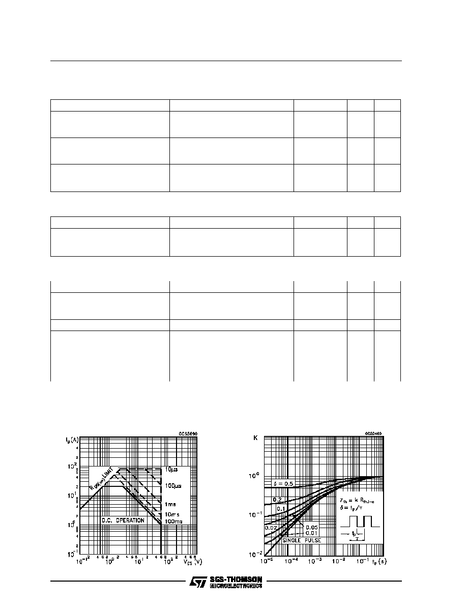
Safe Operating Area
Thermal Impedance
STD20N06
3/10
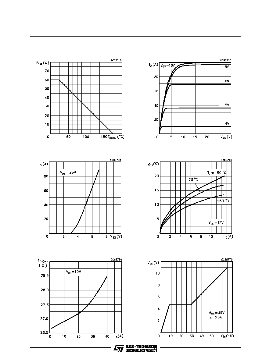
Derating Curve
Transfer Characteristics
Static Drain-source On Resistance
Output Characteristics
Transconductance
Gate Charge vs Gate-source Voltage
STD20N06
4/10
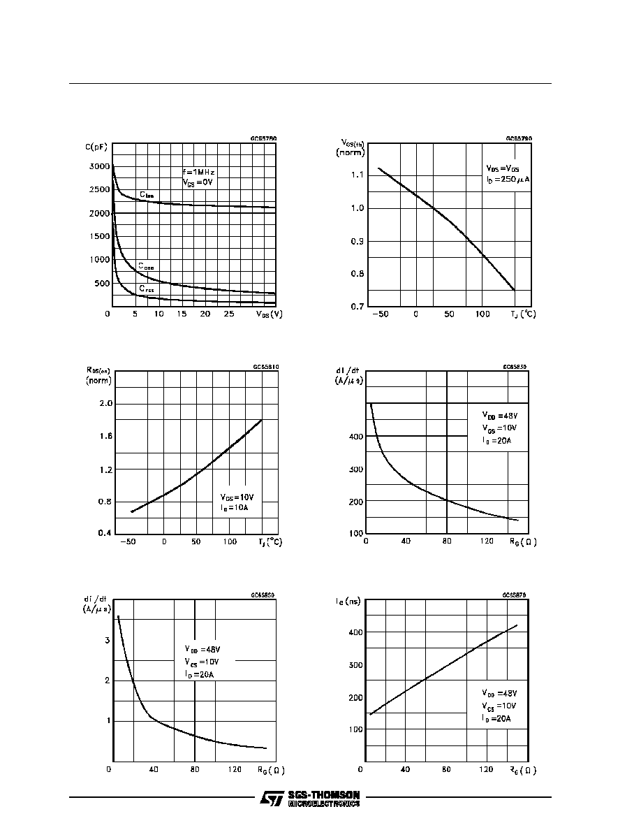
Capacitance Variations
Normalized Gate Threshold Voltage vs
Temperature
Normalized On Resistance vs Temperature
Turn-on Current Slope
Cross-over Time
Turn-off Drain-source Voltage Slope
STD20N06
5/10