 | –≠–ª–µ–∫—Ç—Ä–æ–Ω–Ω—ã–π –∫–æ–º–ø–æ–Ω–µ–Ω—Ç: STD2NB25 | –°–∫–∞—á–∞—Ç—å:  PDF PDF  ZIP ZIP |
STD2NB25
N - CHANNEL 250V - 1.7
- 2A - IPAK/DPAK
PowerMESH
TM
MOSFET
s
TYPICAL R
DS(on)
= 1.7
s
EXTREMELY HIGH dv/dt CAPABILITY
s
100% AVALANCHE TESTED
s
VERY LOW INTRINSIC CAPACITANCES
s
GATE CHARGE MINIMIZED
s
FOR SMD DPAK VERSION CONTACT
SALES OFFICE
DESCRIPTION
Using the latest high voltage MESH OVERLAY
TM
process, STMicroelectronics has designed an
advanced family of power MOSFETs with
outstanding performances. The new patent
pending strip layout coupled with the Company's
proprietary edge termination structure, gives the
lowest R
DS(on)
per area, exceptional avalanche
and dv/dt capabilities and unrivalled gate charge
and switching characteristics.
APPLICATIONS
s
SWITCH MODE POWER SUPPLIES (SMPS)
s
DC-AC CONVERTERS FOR WELDING
EQUIPMENT AND UNINTERRUPTIBLE
POWER SUPPLIES AND MOTOR DRIVE
Æ
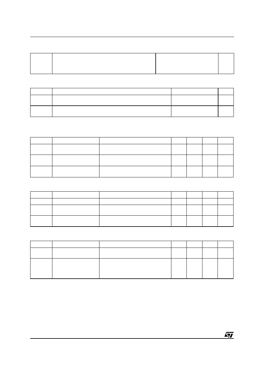
INTERNAL SCHEMATIC DIAGRAM
October 1998
ABSOLUTE MAXIMUM RATINGS
Symbol
Parameter
Value
Unit
V
DS
Drain-source Voltage (V
GS
= 0)
250
V
V
DGR
Drain- gate Voltage (R
GS
= 20 k
)
250
V
V
GS
Gate-source Voltage
±
20
V
I
D
Drain Current (continuous) at T
c
= 25
o
C
2
A
I
D
Drain Current (continuous) at T
c
= 100
o
C
1.25
A
I
DM
(
∑
)
Drain Current (pulsed)
8
A
P
tot
Total Dissipation at T
c
= 25
o
C
40
W
Derating Factor
0.32
W/
o
C
dv/dt(
1
)
Peak Diode Recovery voltage slope
6
V/ns
T
stg
Storage Temperature
-65 to 150
o
C
T
j
Max. Operating Junction Temperature
150
o
C
(
∑
) Pulse width limited by safe operating area (
1
) I
SD
2A, di/dt
200 A/
µ
s, V
DD
V
(BR)DSS
, Tj
T
JMAX
TYPE
V
DSS
R
DS(on)
I
D
STD2NB25
250 V
< 2
2 A
3
2
1
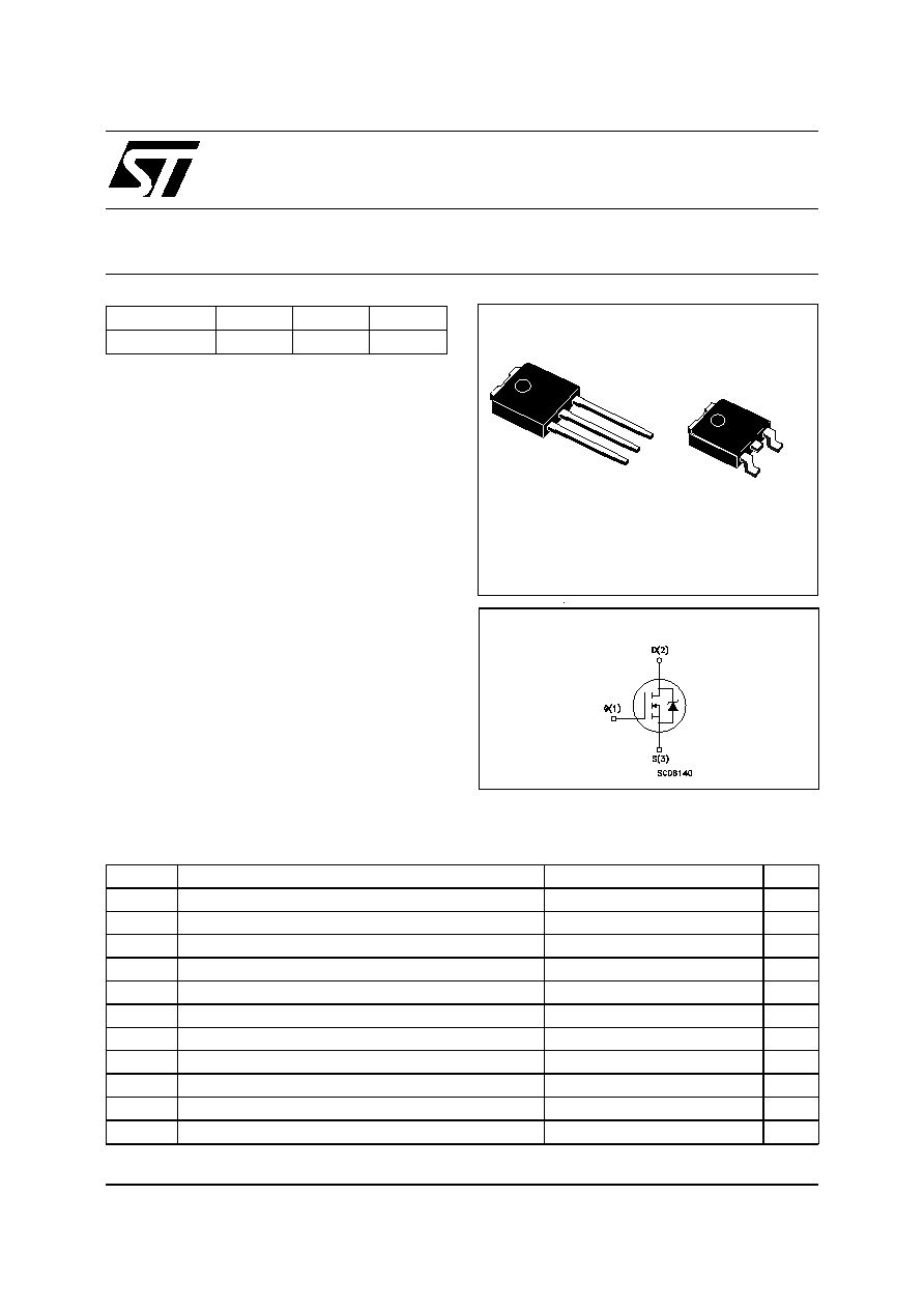
IPAK
TO-251
(Suffix "-1")
1
3
DPAK
TO-252
(Suffix "T4")
1/9
THERMAL DATA
R
thj-case
Rthj-amb
R
thc-sink
T
l
Thermal Resistance Junction-case Max
Thermal Resistance Junction-ambient Max
Thermal Resistance Case-sink Typ
Maximum Lead Temperature For Soldering Purpose
3.12
100
1.5
275
o
C/W
oC/W
o
C/W
o
C
AVALANCHE CHARACTERISTICS
Symbol
Parameter
Max Value
Unit
I
AR
Avalanche Current, Repetitive or Not-Repetitive
(pulse width limited by T
j
max)
2
A
E
AS
Single Pulse Avalanche Energy
(starting T
j
= 25
o
C, I
D
= I
AR
, V
DD
= 50 V)
50
mJ
ELECTRICAL CHARACTERISTICS (T
case
= 25
o
C unless otherwise specified)
OFF
Symbol
Parameter
Test Conditions
Min.
Typ.
Max.
Unit
V
(BR)DSS
Drain-source
Breakdown Voltage
I
D
= 250
µ
A V
GS
= 0
250
V
I
DSS
Zero Gate Voltage
Drain Current (V
GS
= 0)
V
DS
= Max Rating
V
DS
= Max Rating T
c
= 125
o
C
1
10
µ
A
µ
A
I
GSS
Gate-body Leakage
Current (V
DS
= 0)
V
GS
=
±
20 V
±
100
nA
ON (
)
Symbol
Parameter
Test Conditions
Min.
Typ.
Max.
Unit
V
GS(th)
Gate Threshold Voltage V
DS
= V
GS
I
D
= 250
µ
A
2
3
4
V
R
DS(on)
Static Drain-source On
Resistance
V
GS
= 10V I
D
=1 A
1.7
2
I
D(o n)
On State Drain Current
V
DS
> I
D(o n)
x R
DS(on )max
V
GS
= 10 V
2
A
DYNAMIC
Symbol
Parameter
Test Conditions
Min.
Typ.
Max.
Unit
g
fs
(
)
Forward
Transconductance
V
DS
> I
D(o n)
x R
DS(on )max
I
D
= 1 A
0.5
1.6
S
C
iss
C
oss
C
rss
Input Capacitance
Output Capacitance
Reverse Transfer
Capacitance
V
DS
= 25 V f = 1 MHz V
GS
= 0
185
45
5
250
60
7
pF
pF
pF
STD2NB25
2/9
ELECTRICAL CHARACTERISTICS (continued)
SWITCHING ON
Symbol
Parameter
Test Conditions
Min.
Typ.
Max.
Unit
t
d(on )
t
r
Turn-on Time
Rise Time
V
DD
= 125 V I
D
= 1 A
R
G
= 4.7
V
GS
= 10 V
(see test circuit, figure 3)
5
7
7
10
ns
ns
Q
g
Q
gs
Q
gd
Total Gate Charge
Gate-Source Charge
Gate-Drain Charge
V
DD
= 200 V I
D
=2 A V
GS
= 10 V
10.3
3.7
2.3
16
nC
nC
nC
SWITCHING OFF
Symbol
Parameter
Test Conditions
Min.
Typ.
Max.
Unit
t
r(Voff)
t
f
t
c
Off-voltage Rise Time
Fall Time
Cross-over Time
V
DD
= 200 V I
D
= 2 A
R
G
= 4.7
V
GS
= 10 V
(see test circuit, figure 5)
11
13
18
15
18
24
ns
ns
ns
SOURCE DRAIN DIODE
Symbol
Parameter
Test Conditions
Min.
Typ.
Max.
Unit
I
SD
I
SDM
(
∑
)
Source-drain Current
Source-drain Current
(pulsed)
2
8
A
A
V
SD
(
)
Forward On Voltage
I
SD
= 2 A V
GS
= 0
1.5
V
t
rr
Q
rr
I
RRM
Reverse Recovery
Time
Reverse Recovery
Charge
Reverse Recovery
Current
I
SD
= 2 A di/dt = 100 A/
µ
s
V
DD
= 50 V T
j
= 150
o
C
(see test circuit, figure 5)
120
300
5
ns
nC
A
(
) Pulsed: Pulse duration = 300
µ
s, duty cycle 1.5 %
(
∑
) Pulse width limited by safe operating area
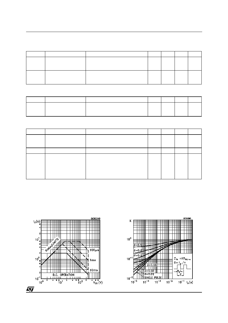
Safe Operating Area
Thermal Impedance
STD2NB25
3/9
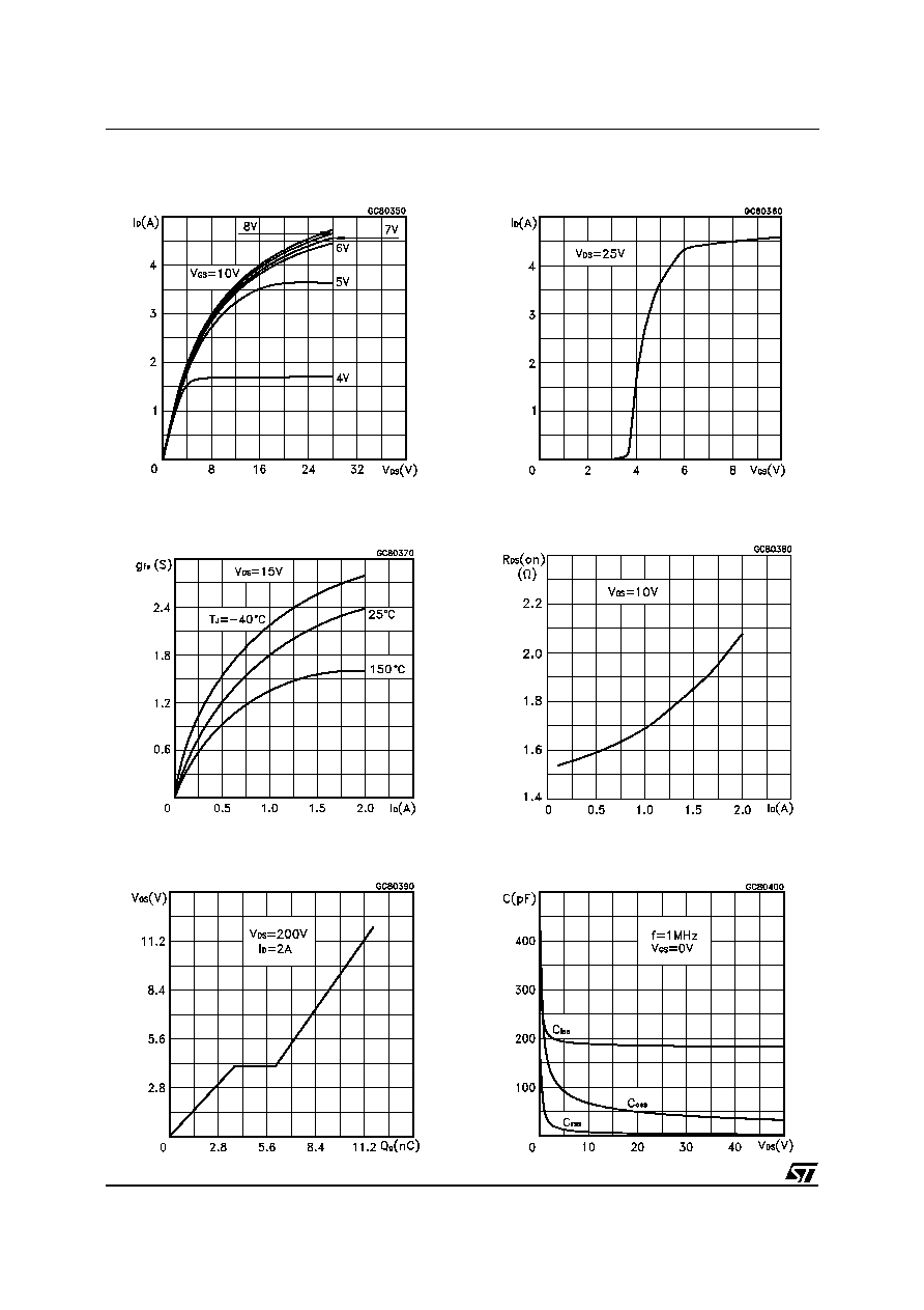
Output Characteristics
Transconductance
Gate Charge vs Gate-source Voltage
Transfer Characteristics
Static Drain-source On Resistance
Capacitance Variations
STD2NB25
4/9
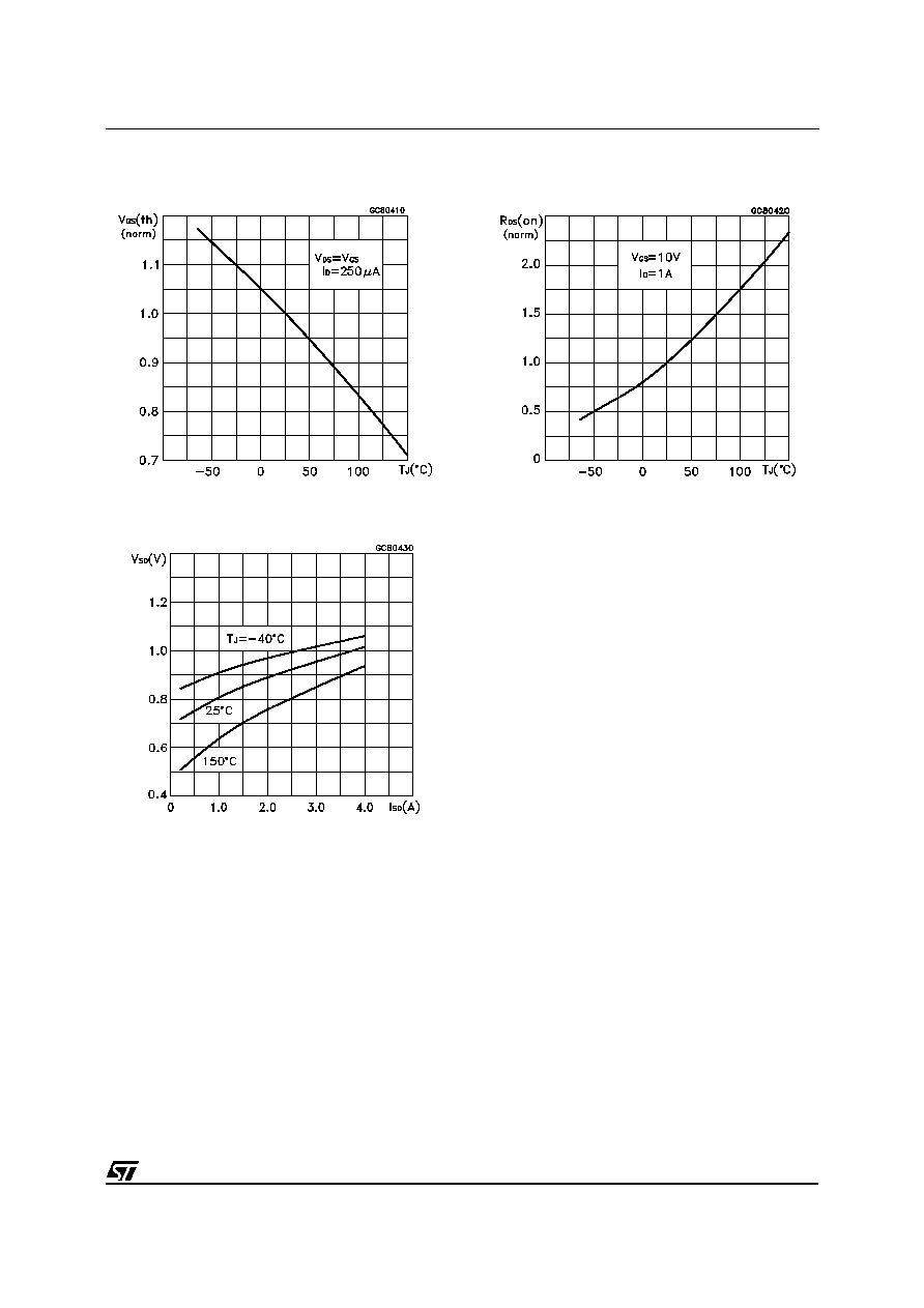
Normalized Gate Threshold Voltage vs
Temperature
Source-drain Diode Forward Characteristics
Normalized On Resistance vs Temperature
STD2NB25
5/9