1/8
May 2000
This is preliminary information on a new product now in development or undergoing evaluation. Details are subject to change without notice.
STD2NC40-1
N-CHANNEL 400V - 4.7
- 1.5A IPAK
PowerMesh
TM
II MOSFET
(1)I
SD
1.5A, di/dt
100A/
µ
s, V
DD
V
(BR)DSS
, T
j
T
JMAX.
s
TYPICAL R
DS
(on) = 4.7
s
EXTREMELY HIGH dv/dt CAPABILITY
s
100% AVALANCHE TESTED
s
NEW HIGH VOLTAGE BENCHMARK
s
GATE CHARGE MINIMIZED
DESCRIPTION
The PowerMESH
TM
II is the evolution of the first
generation of MESH OVERLAY
TM
.
The layout re-
finements introduced greatly improve the Ron*area
figure of merit while keeping the device at the lead-
ing edge for what concerns swithing speed, gate
charge and ruggedness.
APPLICATIONS
s
SWITH MODE LOW POWER SUPPLIES
(SMPS)
s
CFL
ABSOLUTE MAXIMUM RATINGS
(
∑
)Pulse width limite d by safe operating area
TYPE
V
DSS
R
DS(on)
I
D
STD2NC40-1
400V
<5.5
1.5A
Symbol
Parameter
Value
Unit
V
DS
Drain-source Voltage (V
GS
= 0)
400
V
V
DGR
Drain-gate Voltage (R
GS
= 20 k
)
400
V
V
GS
Gate- source Voltage
±
30
V
I
D
Drain Current (continuos) at T
C
= 25
∞
C
1.5
A
I
D
Drain Current (continuos) at T
C
= 100
∞
C
0.95
A
I
DM
(
s
)
Drain Current (pulsed)
6
A
P
TOT
Total Dissipation at T
C
= 25
∞
C
30
W
Derating Factor
0.24
W/
∞
C
dv/dt
Peak Diode Recovery voltage slope
4.5
V/ns
T
stg
Storage Temperature
≠60 to 150
∞
C
T
j
Max. Operating Junction Temperature
150
∞
C
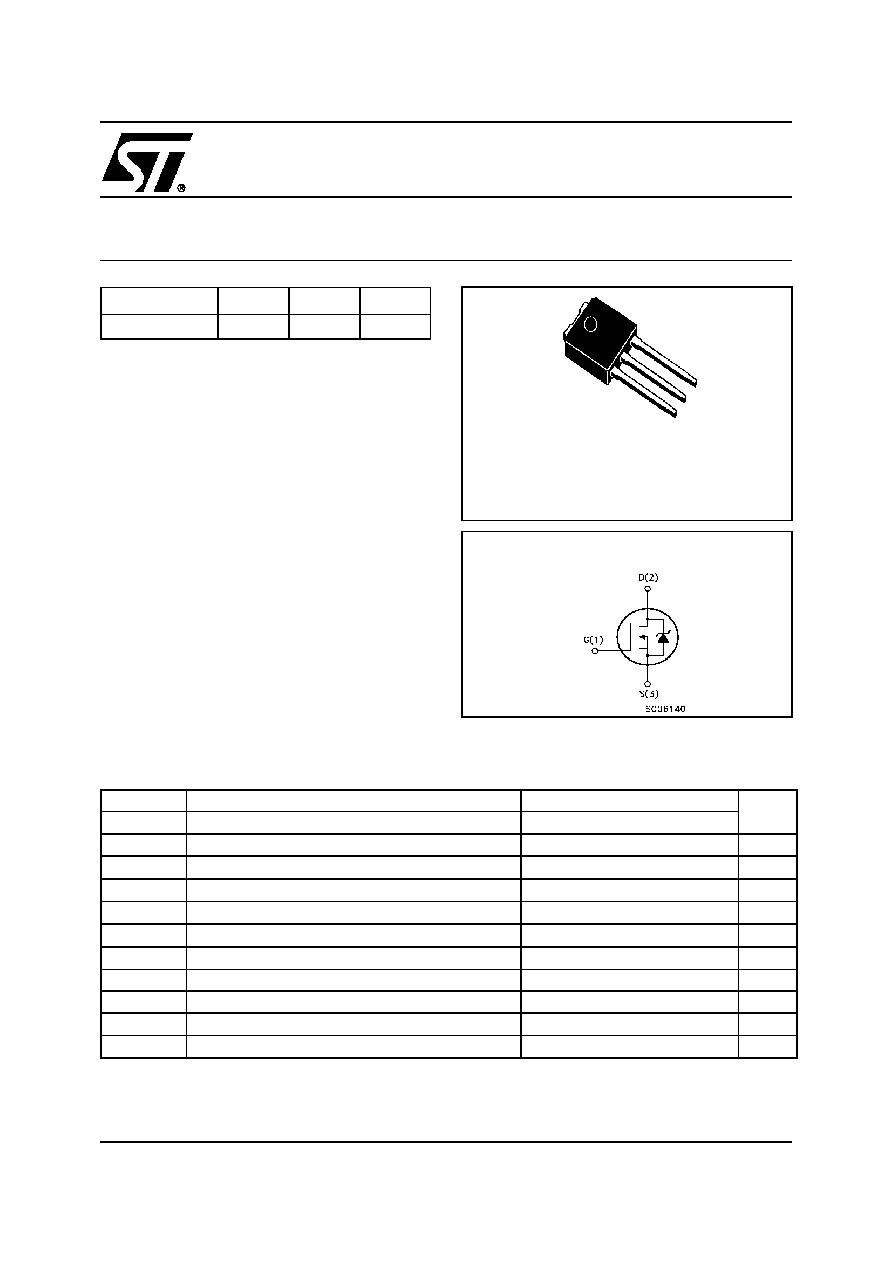
IPAK
(SUFFIX"-1")
3
2
1
INTERNAL SCHEMATIC DIAGRAM
STD2NC40-1
2/8
THERMAL DATA
AVALANCHE CHARACTERISTICS
ELECTRICAL CHARACTERISTICS (TCASE = 25
∞
C UNLESS OTHERWISE SPECIFIED)
OFF
ON (1)
DYNAMIC
Rthj-case
Thermal Resistance Junction-case Max
4.16
∞
C/W
Rthj-amb
Thermal Resistance Junction-ambient Max
100
∞
C/W
Rthc-sink
Thermal Resistance Case-sink Typ
1.5
∞
C/W
T
l
Maximum Lead Temperature For Soldering Purpose
275
∞
C
Symbol
Parameter
Max Value
Unit
I
AR
Avalanche Current, Repetitive or Not-Repetitive
(pulse width limited by T
j
max)
1.5
A
E
AS
Single Pulse Avalanche Energy
(starting T
j
= 25
∞
C, I
D
= I
AR
, V
DD
= 50 V)
125
mJ
Symbol
Parameter
Test Conditions
Min.
Typ.
Max.
Unit
V
(BR)DSS
Drain-source
Breakdown Voltage
I
D
= 250
µ
A, V
GS
= 0
400
V
I
DSS
Zero Gate Voltage
Drain Current (V
GS
= 0)
V
DS
= Max Rating
1
µ
A
V
DS
= Max Rating, T
C
= 125
∞
C
50
µ
A
I
GSS
Gate-body Leakage
Current (V
DS
= 0)
V
GS
=
±
30V
±
100
nA
Symbol
Parameter
Test Conditions
Min.
Typ.
Max.
Unit
V
GS(th)
Gate Threshold Voltage
V
DS
= V
GS
, I
D
= 250
µ
A
2
3
4
V
R
DS(on)
Static Drain-source On
Resistance
V
GS
= 10V, I
D
= 0.7 A
4.7
5.5
I
D(on)
On State Drain Current
V
DS
> I
D(on)
x R
DS(on)max,
V
GS
= 10V
1.5
A
Symbol
Parameter
Test Conditions
Min.
Typ.
Max.
Unit
g
fs
(1)
Forward Transconductance
V
DS
> I
D(on)
x R
DS(on)max,
I
D
=0.7A
1.1
S
C
iss
Input Capacitance
V
DS
= 25V, f = 1 MHz, V
GS
= 0
108
pF
C
oss
Output Capacitance
22.5
pF
C
rss
Reverse Transfer
Capacitance
0.4
pF
3/8
STD2NC40-1
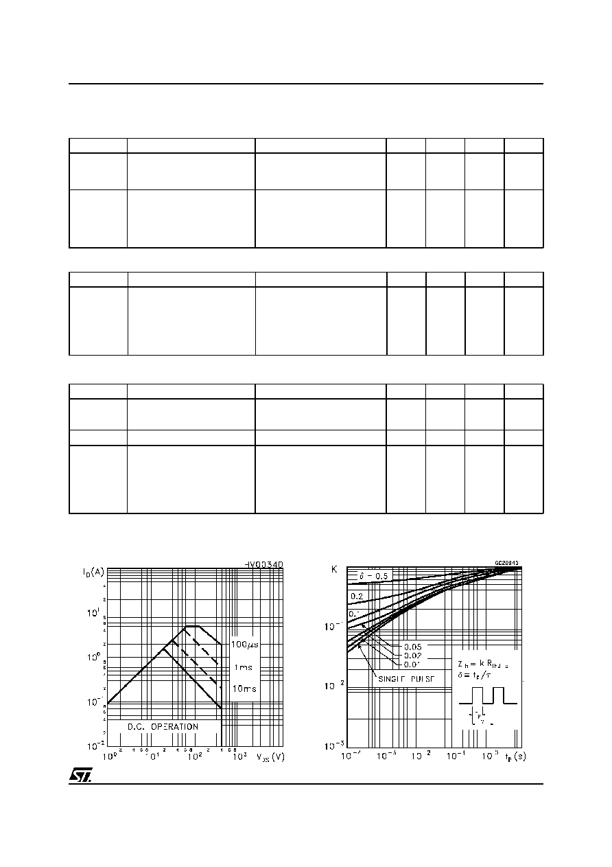
Thermal Impedence
Safe Operating Area
ELECTRICAL CHARACTERISTICS (CONTINUED)
SWITCHING ON
SWITCHING OFF
SOURCE DRAIN DIODE
Note: 1. Pulsed: Pulse duration = 300
µ
s, duty cycle 1.5 %.
2. Pulse width limited by safe operating area.
Symbol
Parameter
Test Conditions
Min.
Typ.
Max.
Unit
t
d(on)
Turn-on Delay Time
V
DD
= 200V, I
D
= 0.7A
R
G
= 4.7
V
GS
= 10V
(see test circuit, Figure 3)
7.5
ns
t
r
Rise Time
12
ns
Q
g
Total Gate Charge
V
DD
= 320V, ID = 1.5A,
V
GS
= 10V
6.1
8.2
nC
Q
gs
Gate-Source Charge
2.1
nC
Q
gd
Gate-Drain Charge
2.4
nC
Symbol
Parameter
Test Condit ions
Min.
Typ.
Max.
Unit
t
r(Voff)
Off-voltage Rise Time
V
DD
= 320V, I
D
= 1.5A,
R
G
= 4.7
,
V
GS
= 10V
(see test circuit, Figure 5)
20
ns
t
f
Fall Time
27
ns
t
c
Cross-over Time
29
ns
Symbol
Parameter
Test Conditions
Min.
Typ.
Max.
Unit
I
SD
Source-drain Current
1.5
A
I
SDM
(1)
Source-drain Current (pulsed)
6
A
V
SD
(2)
Forward On Voltage
I
SD
= 1.5A, V
GS
= 0
1.5
V
t
rr
Reverse Recovery Time
I
SD
= 1.5A, di/dt = 100A/
µ
s,
V
DD
= 100V, T
j
= 150
∞
C
(see test circuit, Figure 5)
180
ns
Q
rr
Reverse Recovery Charge
625
nC
I
RRM
Reverse Recovery Current
5
A
STD2NC40-1
4/8
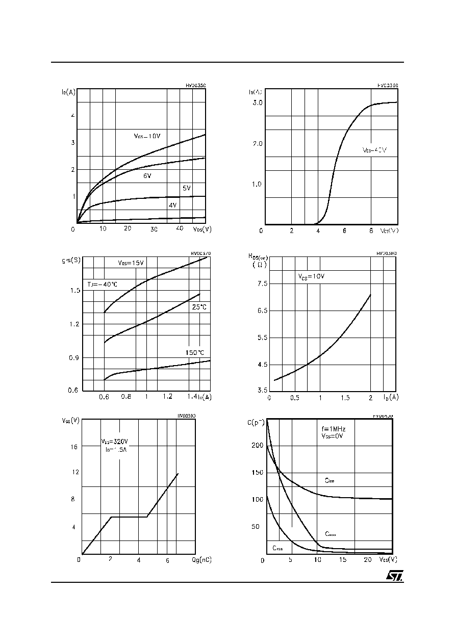
Gate Charge vs Gate-source Voltage
Static Drain-source On Resistance
Transfer Characteristics
Transconductance
Output Characteristics
Capacitance Variations
5/8
STD2NC40-1
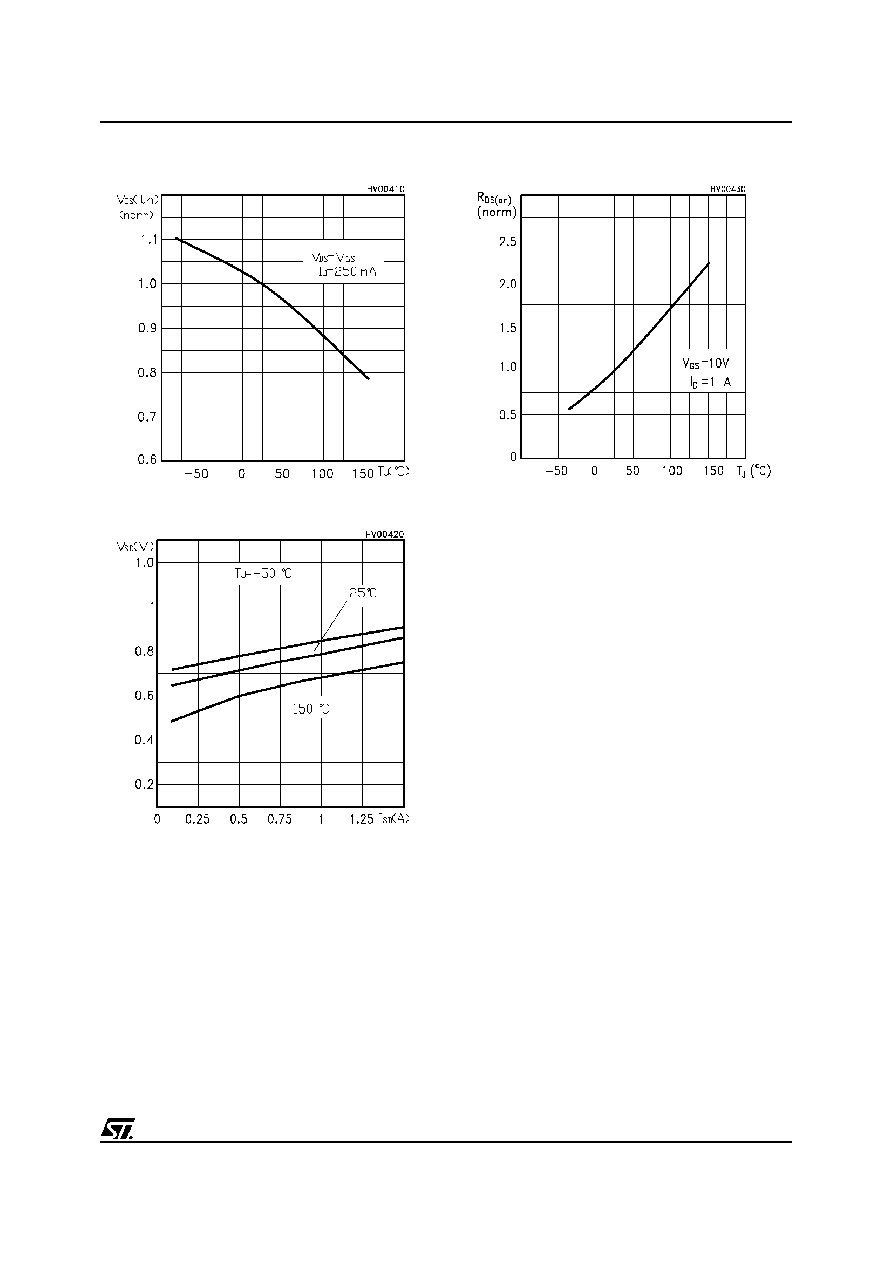
Normalized Gate Threshold Voltage vs
Temperature
Source-drain Diode Forward Characteristics
Normalized On Resistance vs Temperature