 | –≠–ª–µ–∫—Ç—Ä–æ–Ω–Ω—ã–π –∫–æ–º–ø–æ–Ω–µ–Ω—Ç: STD2NC60 | –°–∫–∞—á–∞—Ç—å:  PDF PDF  ZIP ZIP |

1/9
January 2001
STD2NC60
N-CHANNEL 600V - 3.3
- 2A DPAK / IPAK
PowerMeshTMII MOSFET
s
TYPICAL R
DS
(on) = 3.3
s
EXTREMELY HIGH dv/dt CAPABILITY
s
100% AVALANCHE TESTED
s
NEW HIGH VOLTAGE BENCHMARK
s
GATE CHARGE MINIMIZED
DESCRIPTION
The PowerMESH
TM
II is
the evolution of the first
generation of MESH OVERLAY
TM.
The layout re-
finements introduced greatly improve the Ron*area
figure of merit while keeping the device at the lead-
ing edge for what concerns swithing speed, gate
charge and ruggedness.
APPLICATIONS
s
HIGH CURRENT, HIGH SPEED SWITCHING
s
SWITH MODE POWER SUPPLIES (SMPS)
s
DC-AC CONVERTERS FOR WELDING
EQUIPMENT AND UNINTERRUPTIBLE
POWER SUPPLIES AND MOTOR DRIVERS
ABSOLUTE MAXIMUM RATINGS
(∑)Pulse width limited by safe operating area
(1)I
SD
2A, di/dt
100A/µs, V
DD
V
(BR)DSS
, T
j
T
JMAX.
TYPE
V
DSS
R
DS(on)
I
D
STD2NC60
600V
< 3.6
2A
Symbol
Parameter
Value
Unit
V
DS
Drain-source Voltage (V
GS
= 0)
600
V
V
DGR
Drain-gate Voltage (R
GS
= 20 k
)
600
V
V
GS
Gate- source Voltage
±30
V
I
D
Drain Current (continuos) at T
C
= 25∞C
2
A
I
D
Drain Current (continuos) at T
C
= 100∞C
1.3
A
I
DM
(
q
)
Drain Current (pulsed)
8
A
P
TOT
Total Dissipation at T
C
= 25∞C
60
W
Derating Factor
0.48
W/∞C
dv/dt(1)
Peak Diode Recovery voltage slope
4
V/ns
T
stg
Storage Temperature
≠65 to 150
∞C
T
j
Max. Operating Junction Temperature
150
∞C
3
2
1
1
3
DPAK
IPAK
INTERNAL SCHEMATIC DIAGRAM
STD2NC60
2/9
THERMAL DATA
AVALANCHE CHARACTERISTICS
ELECTRICAL CHARACTERISTICS (TCASE = 25 ∞C UNLESS OTHERWISE SPECIFIED)
OFF
ON
(1)
DYNAMIC
Rthj-case
Thermal Resistance Junction-case Max
2
∞C/W
Rthj-amb
Thermal Resistance Junction-ambient Max
100
∞C/W
T
l
Maximum Lead Temperature For Soldering Purpose
275
∞C
Symbol
Parameter
Max Value
Unit
I
AR
Avalanche Current, Repetitive or Not-Repetitive
(pulse width limited by T
j
max)
2
A
E
AS
Single Pulse Avalanche Energy
(starting T
j
= 25 ∞C, I
D
= I
AR
, V
DD
= 50 V)
80
mJ
Symbol
Parameter
Test Conditions
Min.
Typ.
Max.
Unit
V
(BR)DSS
Drain-source
Breakdown Voltage
I
D
= 250 µA, V
GS
= 0
600
V
I
DSS
Zero Gate Voltage
Drain Current (V
GS
= 0)
V
DS
= Max Rating
1
µA
V
DS
= Max Rating, T
C
= 125 ∞C
50
µA
I
GSS
Gate-body Leakage
Current (V
DS
= 0)
V
GS
= ±30V
±100
nA
Symbol
Parameter
Test Conditions
Min.
Typ.
Max.
Unit
V
GS(th)
Gate Threshold Voltage
V
DS
= V
GS
, I
D
= 250µA
2
3
4
V
R
DS(on)
Static Drain-source On
Resistance
V
GS
= 10V, I
D
= 1.5 A
3.3
3.6
I
D(on)
On State Drain Current
V
DS
> I
D(on)
x R
DS(on)max,
V
GS
= 10V
2
A
Symbol
Parameter
Test Conditions
Min.
Typ.
Max.
Unit
g
fs
(1)
Forward Transconductance
V
DS
> I
D(on)
x R
DS(on)max,
I
D
= 1.5A
1.2
2
S
C
iss
Input Capacitance
V
DS
= 25V, f = 1 MHz, V
GS
= 0
400
pF
C
oss
Output Capacitance
57
pF
C
rss
Reverse Transfer
Capacitance
7
pF
3/9
STD2NC60
ELECTRICAL CHARACTERISTICS (CONTINUED)
SWITCHING ON
SWITCHING OFF
SOURCE DRAIN DIODE
Note: 1. Pulsed: Pulse duration = 300 µs, duty cycle 1.5 %.
2. Pulse width limited by safe operating area.
Symbol
Parameter
Test Conditions
Min.
Typ.
Max.
Unit
t
d(on)
Turn-on Delay Time
V
DD
= 300V, I
D
= 1.5A
R
G
= 4.7
V
GS
= 10V
(see test circuit, Figure 3)
13
ns
t
r
Rise Time
9
ns
Q
g
Total Gate Charge
V
DD
= 480V, I
D
= 3A,
V
GS
= 10V
15
22
nC
Q
gs
Gate-Source Charge
6.2
nC
Q
gd
Gate-Drain Charge
5.6
nC
Symbol
Parameter
Test Conditions
Min.
Typ.
Max.
Unit
t
r(Voff)
Off-voltage Rise Time
V
DD
= 480V, I
D
= 3A,
R
G
= 4.7
,
V
GS
= 10V
(see test circuit, Figure 5)
11
ns
t
f
Fall Time
13
ns
t
c
Cross-over Time
18
ns
Symbol
Parameter
Test Conditions
Min.
Typ.
Max.
Unit
I
SD
Source-drain Current
2
A
I
SDM
(2)
Source-drain Current (pulsed)
8
A
V
SD
(1)
Forward On Voltage
I
SD
= 3A, V
GS
= 0
1.6
V
t
rr
Reverse Recovery Time
I
SD
= 3A, di/dt = 100A/µs,
V
DD
= 100V, T
j
= 150∞C
(see test circuit, Figure 5)
500
ns
Q
rr
Reverse Recovery Charge
2.1
µC
I
RRM
Reverse Recovery Current
8.5
A
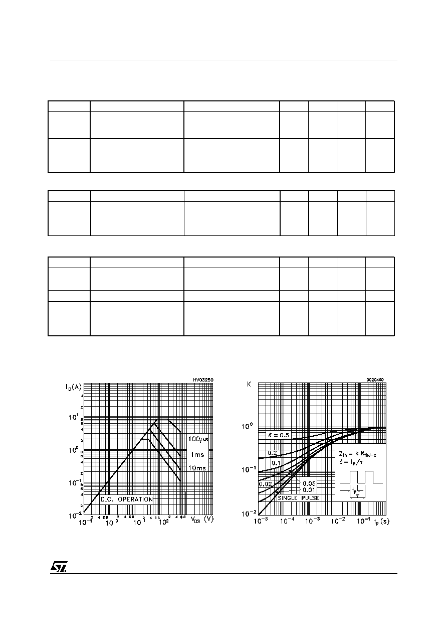
Thermal Impedance
Safe Operating Area
STD2NC60
4/9
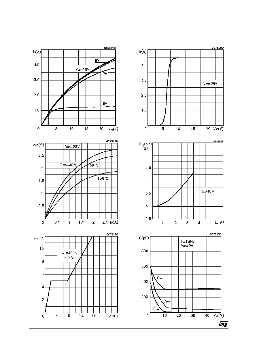
Capacitance Variations
Output Characteristics
Tranconductance
Gate Charge vs Gate-source Voltage
Tranfer Characteristics
Static Drain-Source On Resistance
5/9
STD2NC60
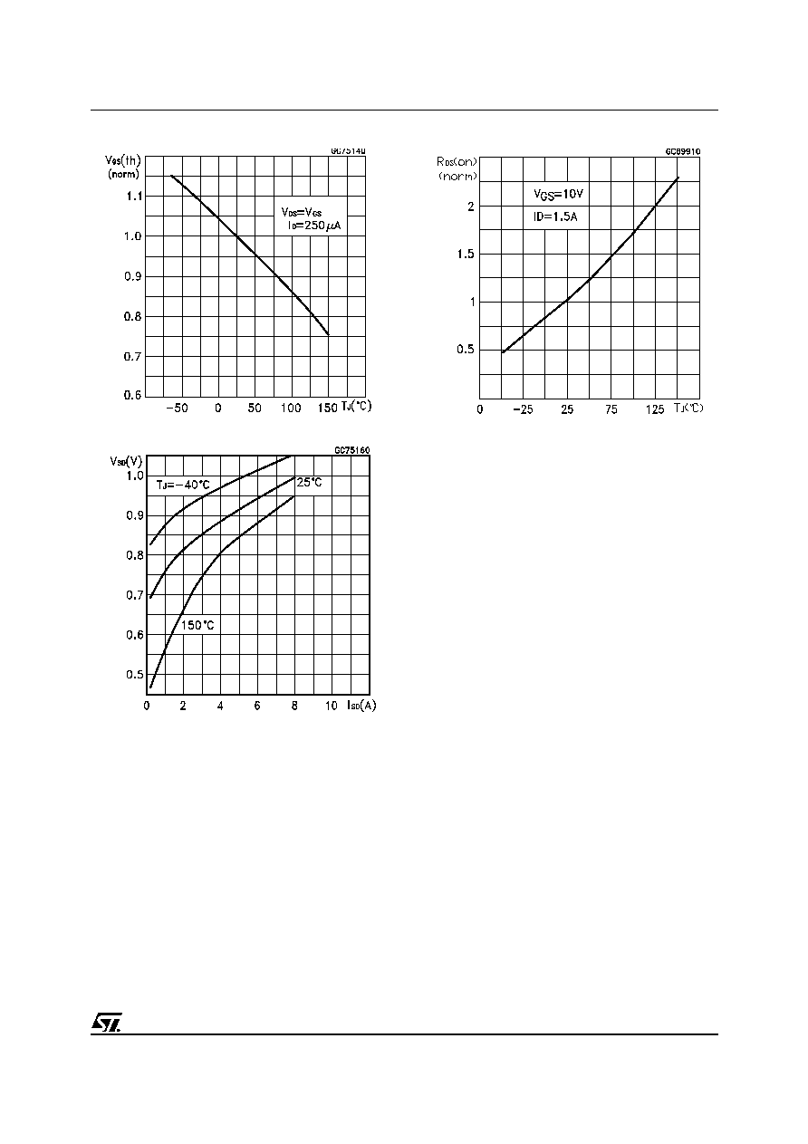
Normalized On Resistance vs Temperature
Normalized Gate Thereshold Voltage vs Temp.
Source-drain Diode Forward Characteristics
STD2NC60
6/9
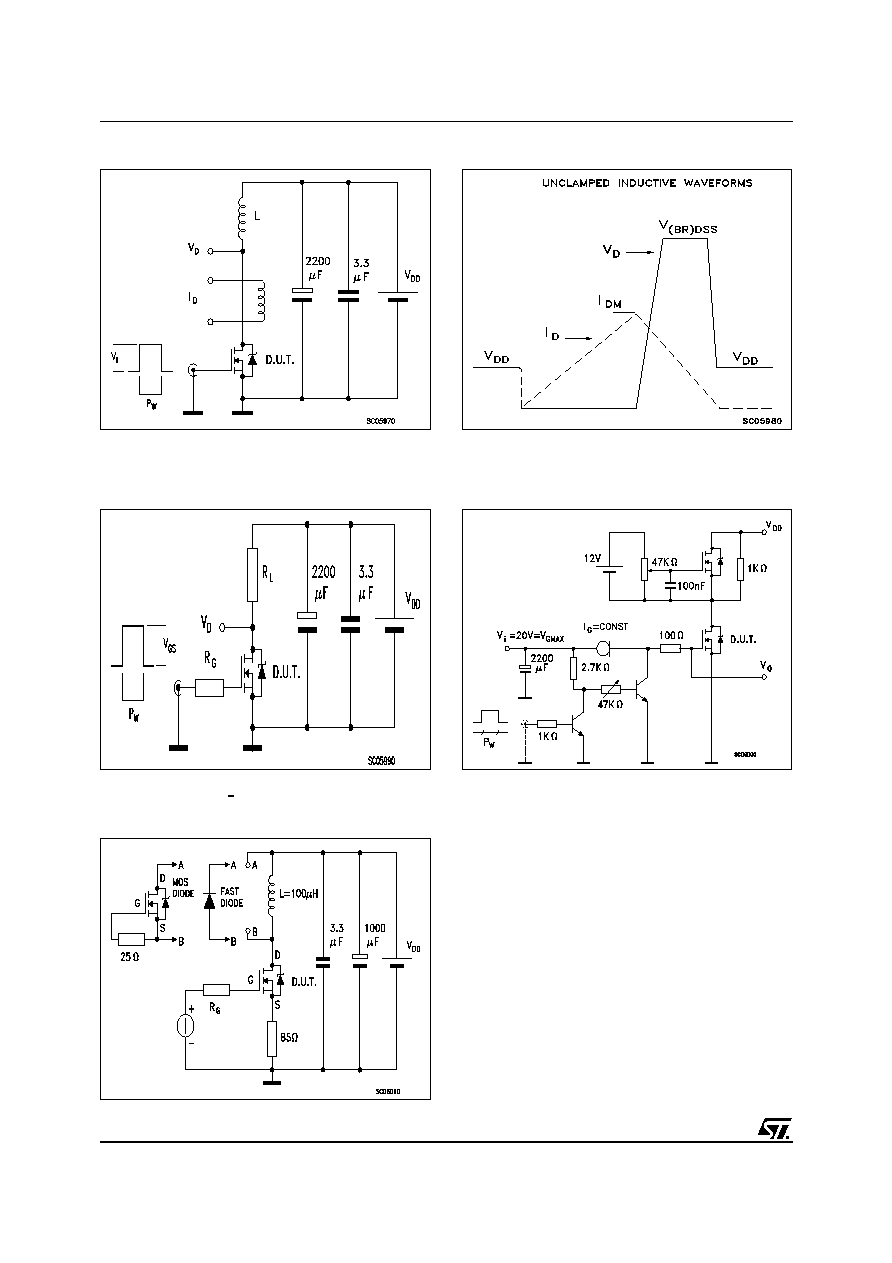
Fig. 5: Test Circuit For Inductive Load Switching
And Diode Recovery Times
Fig. 4: Gate Charge test Circuit
Fig. 2: Unclamped Inductive Waveform
Fig. 1: Unclamped Inductive Load Test Circuit
Fig. 3: Switching Times Test Circuits For
Resistive Load
7/9
STD2NC60
DIM.
mm
inch
MIN.
TYP.
MAX.
MIN.
TYP.
MAX.
A
2.2
2.4
0.086
0.094
A1
0.9
1.1
0.035
0.043
A3
0.7
1.3 0.027
0.051
B
0.64
0.9
0.025
0.031
B2
5.2
5.4
0.204
0.212
B3
0.85
0.033
B5
0.3
0.012
B6
0.95
0.037
C
0.45
0.6
0.017
0.023
C2
0.48
0.6
0.019
0.023
D
6
6.2
0.236
0.244
E
6.4
6.6
0.252
0.260
G
4.4
4.6
0.173
0.181
H
15.9
16.3
0.626
0.641
L
9
9.4
0.354
0.370
L1
0.8
1.2
0.031
0.047
L2
0.8
1
0.031
0.039
A
C2
C
A3
H
A1
D
L
L2
L1
1 3
= =
B3
B
B6
B2
E
G
= =
= =
B5
2
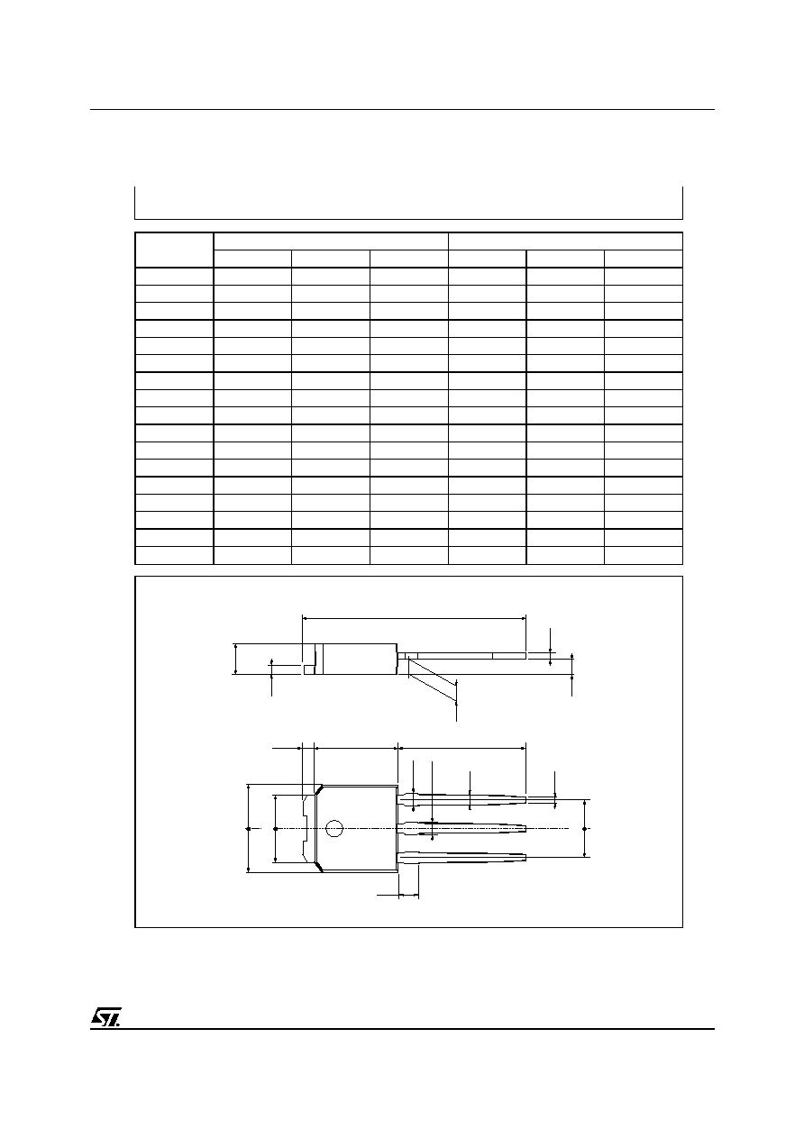
TO-251 (IPAK) MECHANICAL DATA
0068771-E
STD2NC60
8/9
DIM.
mm
inch
MIN.
TYP.
MAX.
MIN.
TYP.
MAX.
A
2.20
2.40
0.087
0.094
A1
0.90
1.10
0.035
0.043
A2
0.03
0.23
0.001
0.009
B
0.64
0.90
0.025
0.035
B2
5.20
5.40
0.204
0.213
C
0.45
0.60
0.018
0.024
C2
0.48
0.60
0.019
0.024
D
6.00
6.20
0.236
0.244
E
6.40
6.60
0.252
0.260
G
4.40
4.60
0.173
0.181
H
9.35
10.10
0.368
0.398
L2
0.8
0.031
L4
0.60
1.00
0.024
0.039
V2
0
o
8
o
0
o
0
o
P032P_B
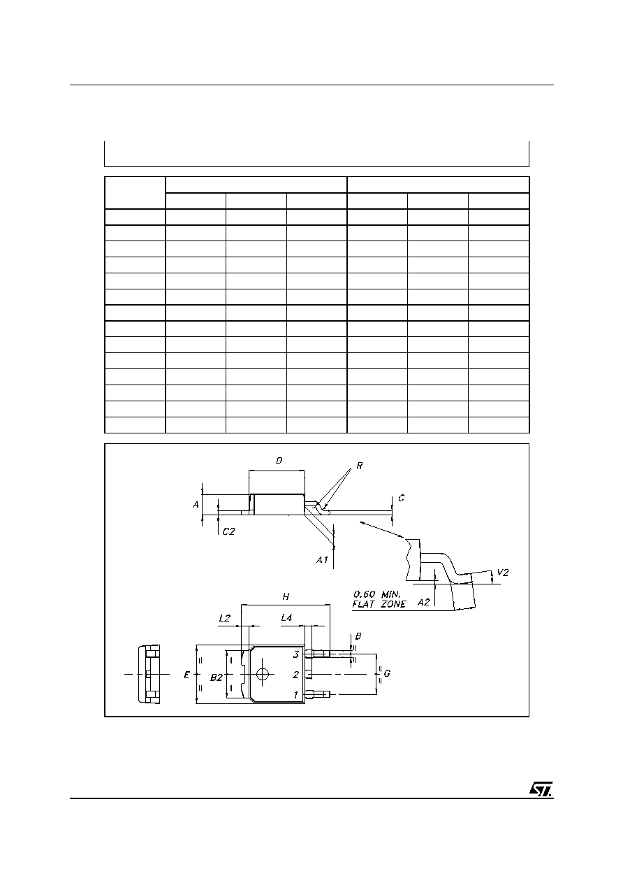
TO-252 (DPAK) MECHANICAL DATA

9/9
STD2NC60
Information furnished is believed to be accurate and reliable. However, STMicroelectronics assumes no responsibility for the consequences
of use of such information nor for any infringement of patents or other rights of third parties which may result from its use. No license is
granted by implication or otherwise under any patent or patent rights of STMicroelectronics. Specification mentioned in this publication are
subject to change without notice. This publication supersedes and replaces all information previously supplied. STMicroelectronics products
are not authorized for use as critical components in life support devices or systems without express written approval of STMicroelectronics.
The ST logo is a trademark of STMicroelectronics
© 2000 STMicroelectronics ≠ Printed in Italy ≠ All Rights Reserved
STMicroelectronics GROUP OF COMPANIES
Australia - Brazil - China - Finland - France - Germany - Hong Kong - India - Italy - Japan - Malaysia - Malta - Morocco -
Singapore - Spain - Sweden - Switzerland - United Kingdom - U.S.A.
http://www.st.com