 | ÐлекÑÑоннÑй компоненÑ: STD2NK70Z | СкаÑаÑÑ:  PDF PDF  ZIP ZIP |
Äîêóìåíòàöèÿ è îïèñàíèÿ www.docs.chipfind.ru
1/12
January 2005
STD2NK70Z - STD2NK70Z-1
N-CHANNEL 700 V - 6
- 1.6 A DPAK/IPAK
Zener-Protected SuperMESHTM MOSFET
Table 1: General Features
s
TYPICAL R
DS
(on) = 6
s
EXTREMELY HIGH dv/dt CAPABILITY
s
ESD IMPROVED CAPABILITY
s
100% AVALANCHE TESTED
s
NEW HIGH VOLTAGE BENCHMARK
s
GATE CHARGE MINIMIZED
DESCRIPTION
The SuperMESHTM
series is obtained through an
extreme optimization of ST's well established
strip-based PowerMESHTM layout. In addition to
pushing on-resistance significantly down, special
care is taken to ensure a very good dv/dt capability
for the most demanding application. Such series
complements ST full range of high vltage MOS-
FETs including revolutionary MDmeshTM products.
APPLICATIONS
s
SINGLE-ENDED SMPS IN MONITORS,
COMPUTER AND INDUSTRIAL
APPLICATION
s
WELDING EQUIPMENT
s
FLYBACK CONFIGURATION FOR BATTERY
CHARGER
Table 2: Order Codes
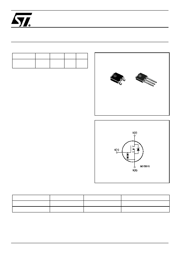
Figure 1: Package
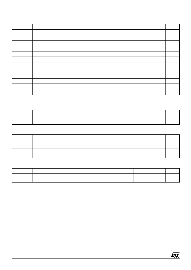
Figure 2: Internal Schematic Diagram
TYPE
V
DSS
R
DS(on)
I
D
Pw
STD2NK70Z
STD2NK70Z-1
700 V
700 V
7
7
1.6 A
1.6 A
45 W
45 W
1
3
3
2
1
DPAK
IPAK
Sales Type
Marking
Package
Packaging
STD2NK70ZT4
D2NK70Z
DPAK
TAPE & REEL
STD2NK70Z-1
D2NK70Z
IPAK
TUBE
Rev. 2
STD2NK70Z - STD2NK70Z-1
2/12
Table 3: Absolute Maximum ratings
(*) Pulse width limited by safe operating area
(1) I
SD
1.6 A, di/dt
200 A/µs, VDD
V
(BR)DSS
Table 4: Thermal Data
Table 5: Avalanche Characteristics
Table 6: Gate-Source Zener Diode
PROTECTION FEATURES OF GATE-TO-SOURCE ZENER DIODES
The built-in back-to-back Zener diodes have specifically been designed to enhance not only the device's
ESD capability, but also to make them safely absorb possible voltage transients that may occasionally be
applied from gate to source. In this respect the Zener voltage is appropriate to achieve an efficient and
cost-effective intervention to protect the device's integrity. These integrated Zener diodes thus avoid the
usage of external components.
Symbol
Parameter
Value
Unit
V
DS
Drain-source Voltage (V
GS
= 0)
700
V
V
DGR
Drain-gate Voltage (R
GS
= 20 K
)
700
V
V
GS
Gate- source Voltage
±
30
V
I
D
Drain Current (continuous) at T
C
= 25°C 1.6
A
I
D
Drain Current (continuous) at T
C
= 100°C
1
A
I
DM
(*)
Drain Current (pulsed)
6.4
A
P
TOT
Total Dissipation at T
C
= 25°C
45
W
Derating Factor
0.36
W/°C
V
ESD(G-S)
Gate source ESD (HBM-C = 100pF, R = 1.5 K
)
2000
V
dv/dt (1)
Peak Diode Recovery voltage slope
4.5
V/ns
T
stg
Storage Temperature
-55 to 150
°C
T
j
Max. Operating Junction Temperature
Rthj-case
Thermal Resistance Junction-case Max
2.78
°C/W
Rthj-amb
T
l
Thermal Resistance Junction-ambient Max
Maximum Lead Temperature For Soldering Purpose
100
300
°C/W
°C
Symbol
Parameter
Max Value
Unit
I
AR
Avalanche Current, Repetitive or Not-Repetitive
(pulse width limited by T
j
max)
1.6
A
E
AS
Single Pulse Avalanche Energy
(starting T
j
= 25 °C, I
D
= I
AR
, V
DD
= 50 V)
110
mJ
Symbol
Parameter
Test Condition
Min.
Typ.
Max
Unit
BV
GSO
Gate-Source Breakdown
Voltage
Igs=
±
1mA (Open Drain)
30
A

3/12
STD2NK70Z - STD2NK70Z-1
TABLE 7: ELECTRICAL CHARACTERISTICS (T
CASE
=25°C UNLESS OTHERWISE SPECIFIED)
On /Off
Table 8: Dynamic
Table 9: Source Drain Diode
(1) Pulsed: Pulse duration = 300
µs, duty cycle 1.5%
(2) Pulse width limited by safe operating area
(3) C
oss eq
. is defined as a constant equivalent capacitance giving the same charging time as C
oss
when V
DS
increases from 0 to 80% V
DSS
Symbol
Parameter
Test Conditions
Min.
Typ.
Max.
Unit
V
(BR)DSS
Drain-source Breakdown
Voltage
I
D
= 1 mA, V
GS
= 0
700
V
I
DSS
Zero Gate Voltage
Drain Current (V
GS
= 0)
V
DS
= Max Rating
V
DS
= Max Rating, T
C
= 125°C
1
50
µA
µA
I
GSS
Gate-body Leakage
Current (V
DS
= 0)
V
GS
= ± 20 V
± 10
µA
V
GS(th)
Gate Threshold Voltage
V
DS
= V
GS
, I
D
= 50 µA
3
3.75
4.5
V
R
DS(on)
Static Drain-source On
Resistance
V
GS
= 10 V, I
D
= 0.8 A
6
7
Symbol
Parameter
Test Conditions
Min.
Typ.
Max.
Unit
g
fs
(1)
Forward Transconductance
V
DS
= 15 V
,
I
D
= 0.8 A
1.4
S
C
oss eq.
(3)
Equivalent Output
Capacitance
V
GS
= 0 V, V
DS
= 0 to 560 V
17
C
iss
C
oss
C
rss
Input Capacitance
Output Capacitance
Reverse Transfer
Capacitance
V
DS
= 25 V, f = 1 MHz, V
GS
= 0
280
35
6.5
pF
pF
pF
t
d(on)
t
r
t
d(off)
t
f
Turn-on Delay Time
Rise Time
Turn-off-Delay Time
Fall Time
V
DD
= 350 V, I
D
= 0.8 A,
R
G
= 4.7
,
V
GS
= 10 V
(see Figure 17)
7
17
20
35
ns
ns
ns
ns
Q
g
Q
gs
Q
gd
Total Gate Charge
Gate-Source Charge
Gate-Drain Charge
V
DD
= 560 V, I
D
= 0.8 A,
V
GS
= 10 V
(see Figure 20)
11.4
2
6.8
15
nC
nC
nC
Symbol
Parameter
Test Conditions
Min.
Typ.
Max.
Unit
I
SD
I
SDM
(2)
Source-drain Current
Source-drain Current (pulsed)
1.6
6.4
A
A
V
SD
(1)
Forward On Voltage
I
SD
= 1.6 A, V
GS
= 0
1.6
V
t
rr
Q
rr
I
RRM
Reverse Recovery Time
Reverse Recovery Charge
Reverse Recovery Current
I
SD
= 1.6, di/dt = 100 A/µs
V
DD
=50 V, T
j
= 25°C
(see Figure 18)
334
918
5.5
ns
µC
A
t
rr
Q
rr
I
RRM
Reverse Recovery Time
Reverse Recovery Charge
Reverse Recovery Current
I
SD
= 1.6, di/dt = 100 A/µs
V
DD
= 50 V, T
j
= 150°C
(see Figure 18)
350
1050
6
ns
µC
A
STD2NK70Z - STD2NK70Z-1
4/12
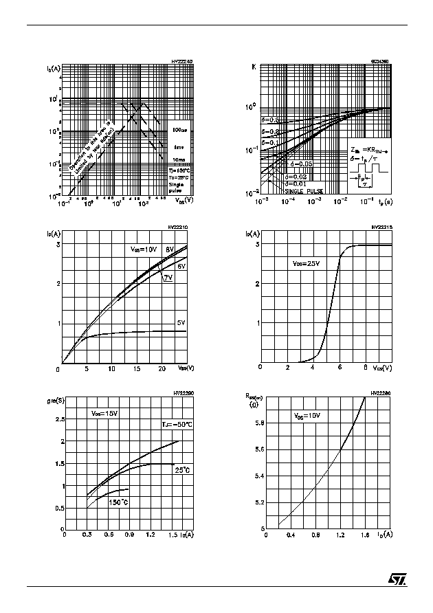
Figure 3: Safe Operating Area
Figure 4: Output Characteristics
Figure 5: Transconductance
Figure 6: Thermal Impedance
Figure 7: Transfer Characteristics
Figure 8: Static Drain-source On Resistance
5/12
STD2NK70Z - STD2NK70Z-1
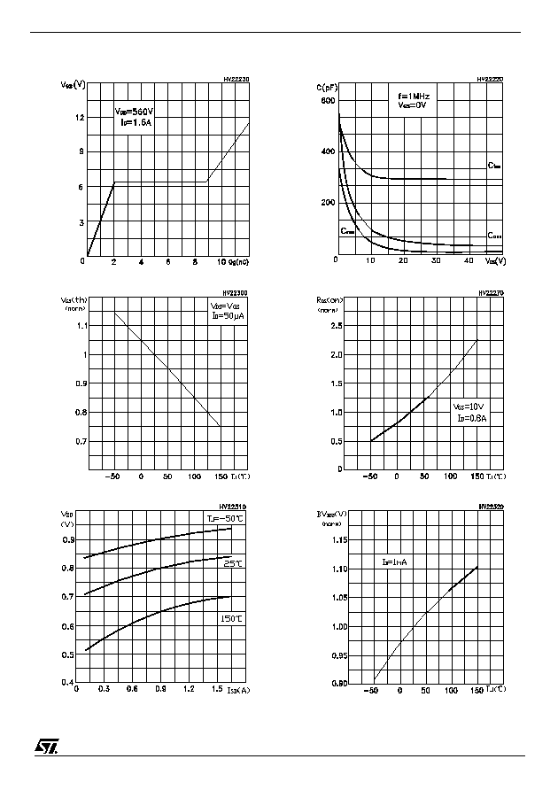
Figure 9: Gate Charge vs Gate-source Voltage
Figure 10: Normalized Gate Thereshold Volt-
age vs Temperature
Figure 11: Dource-Drain Diode Forward Char-
acteristics
Figure 12: Capacitance Variations
Figure 13: Normalized On Resistance vs Tem-
perature
Figure 14: Normalized Breakdown Voltage vs
Temperature
STD2NK70Z - STD2NK70Z-1
6/12
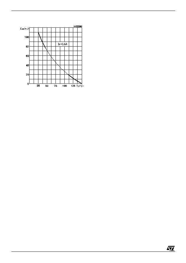
Figure 15: Maximum Avalanche Energy vs
Temperature
7/12
STD2NK70Z - STD2NK70Z-1
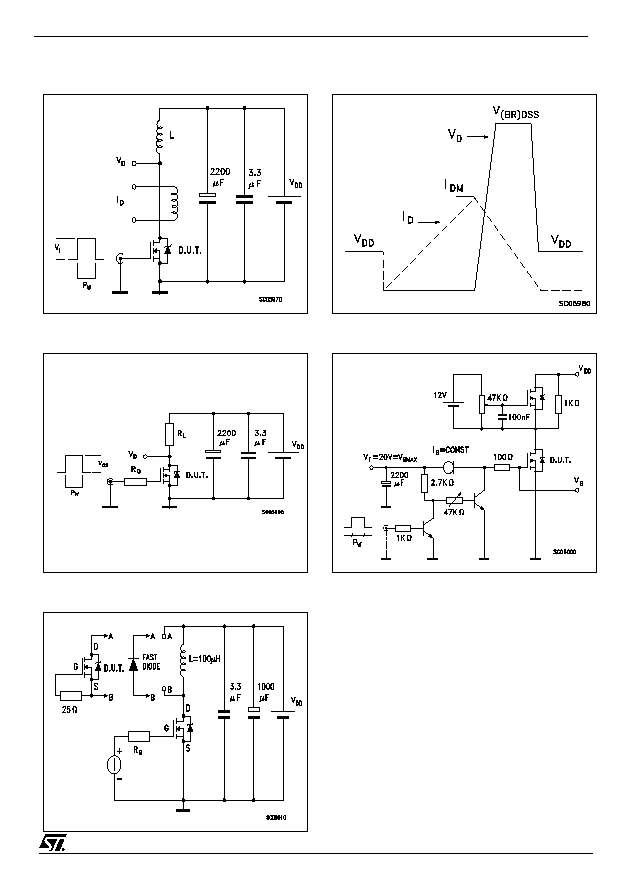
Figure 16: Unclamped Inductive Load Test Cir-
cuit
Figure 17: Switching Times Test Circuit For
Resistive Load
Figure 18: Test Circuit For Inductive Load
Switching and Diode Recovery Times
Figure 19: Unclamped Inductive Wafeform
Figure 20: Gate Charge Test Circuit
STD2NK70Z - STD2NK70Z-1
8/12
DIM.
mm
inch
MIN.
TYP.
MAX.
MIN.
TYP.
MAX.
A
2.20
2.40
0.087
0.094
A1
0.90
1.10
0.035
0.043
A2
0.03
0.23
0.001
0.009
B
0.64
0.90
0.025
0.035
B2
5.20
5.40
0.204
0.213
C
0.45
0.60
0.018
0.024
C2
0.48
0.60
0.019
0.024
D
6.00
6.20
0.236
0.244
E
6.40
6.60
0.252
0.260
G
4.40
4.60
0.173
0.181
H
9.35
10.10
0.368
0.398
L2
0.8
0.031
L4
0.60
1.00
0.024
0.039
V2
0
o
8
o
0
o
0
o
P032P_B
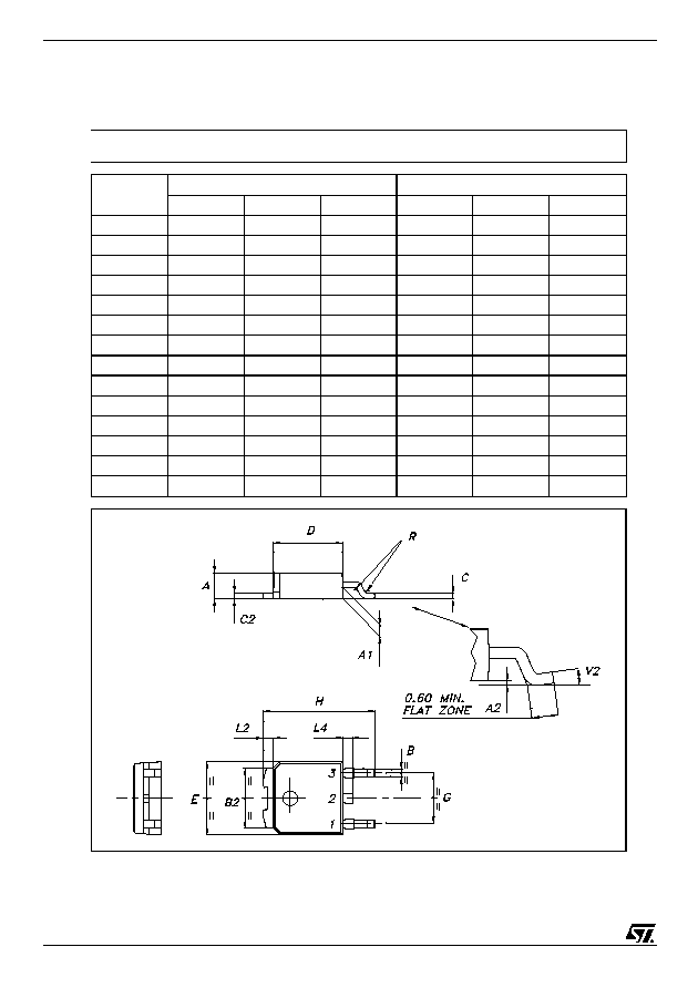
TO-252 (DPAK) MECHANICAL DATA
9/12
STD2NK70Z - STD2NK70Z-1
Information furnished is believed to be accurate and reliable. However, STMicroelectronics assumes no responsibility for the consequences
of use of such information nor for any infringement of patents or other rights of third parties which may result from its use. No license is granted
by implication or otherwise under any patent or patent rights of STMicroelectronics. Specifications mentioned in this publication are subject
to change without notice. This publication supersedes and replaces all information previously supplied. STMicroelectronics products are not
authorized for use as critical components in life support devices or systems without express written approval of STMicroelectronics.
The ST logo is a registered trademark of STMicroelectronics
All other names are the property of their respective owners
© 2005 STMicroelectronics - All Rights Reserved
STMicroelectronics group of companies
Australia - Belgium - Brazil - Canada - China - Czech Republic - Finland - France - Germany - Hong Kong - India - Israel - Italy - Japan -
Malaysia - Malta - Morocco - Singapore - Spain - Sweden - Switzerland - United Kingdom - United States of America
www.st.com
DIM.
mm
inch
MIN.
TYP.
MAX.
MIN.
TYP.
MAX.
A
2.2
2.4
0.086
0.094
A1
0.9
1.1
0.035
0.043
A3
0.7
1.3 0.027
0.051
B
0.64
0.9
0.025
0.031
B2
5.2
5.4
0.204
0.212
B3
0.85
0.033
B5
0.3
0.012
B6
0.95
0.037
C
0.45
0.6
0.017
0.023
C2
0.48
0.6
0.019
0.023
D
6
6.2
0.236
0.244
E
6.4
6.6
0.252
0.260
G
4.4
4.6
0.173
0.181
H
15.9
16.3
0.626
0.641
L
9
9.4
0.354
0.370
L1
0.8
1.2
0.031
0.047
L2
0.8
1
0.031
0.039
A
C2
C
A3
H
A1
D
L
L2
L1
1 3
= =
B3
B
B6
B2
E
G
= =
= =
B5
2
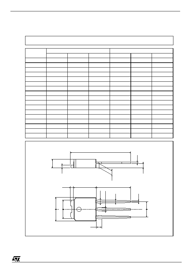
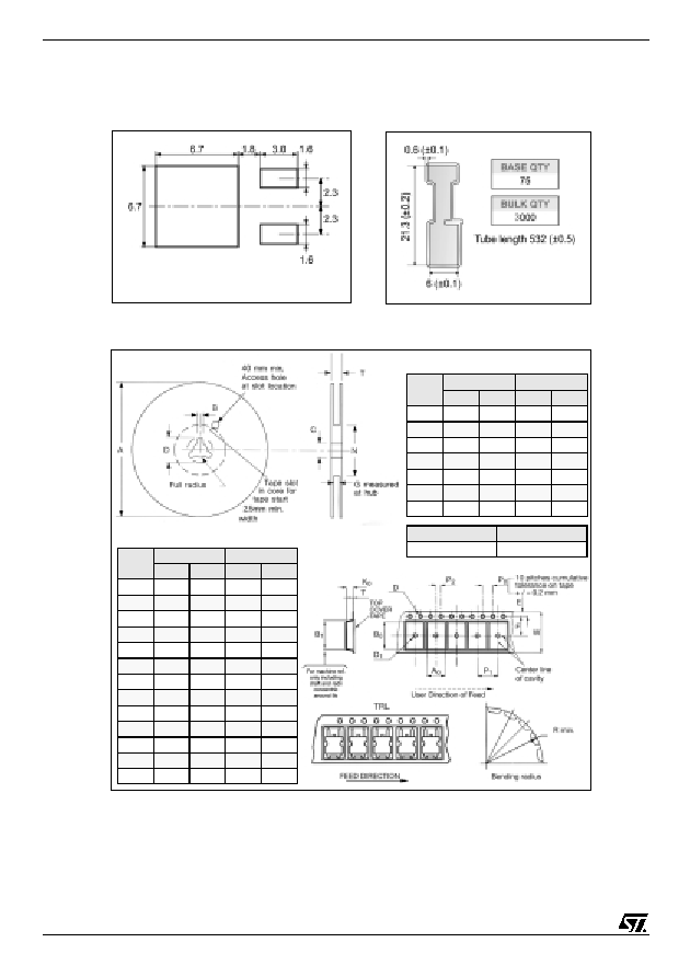
TO-251 (IPAK) MECHANICAL DATA
0068771-E
STD2NK70Z - STD2NK70Z-1
10/12
TAPE AND REEL SHIPMENT (suffix "T4")*
TUBE SHIPMENT (no suffix)*
DPAK FOOTPRINT
* on sales type
DIM.
mm
inch
MIN.
MAX.
MIN.
MAX.
A
330
12.992
B
1.5
0.059
C
12.8
13.2
0.504
0.520
D
20.2
0.795
G
16.4
18.4
0.645
0.724
N
50
1.968
T
22.4
0.881
BASE QTY
BULK QTY
2500
2500
REEL MECHANICAL DATA
DIM.
mm
inch
MIN.
MAX.
MIN.
MAX.
A0
6.8
7
0.267
0.275
B0
10.4
10.6
0.409
0.417
B1
12.1
0.476
D
1.5
1.6
0.059
0.063
D1
1.5
0.059
E
1.65
1.85
0.065
0.073
F
7.4
7.6
0.291
0.299
K0
2.55
2.75
0.100
0.108
P0
3.9
4.1
0.153
0.161
P1
7.9
8.1
0.311
0.319
P2
1.9
2.1
0.075
0.082
R
40
1.574
W
15.7
16.3
0.618
0.641
TAPE MECHANICAL DATA
All dimensions
are in millimeters
All dimensions are in millimeters
11/12
STD2NK70Z - STD2NK70Z-1
Table 10: Revision History
Date
Revision
Description of Changes
07-Sep-2004
1
First Release, complete document.
24-Jan-2005
2
New curve, figure 3, and new Rds(on) value Max.

STD2NK70Z - STD2NK70Z-1
12/12
Information furnished is believed to be accurate and reliable. However, STMicroelectronics assumes no responsibility for the consequences
of use of such information nor for any infringement of patents or other rights of third parties which may result from its use. No license is granted
by implication or otherwise under any patent or patent rights of STMicroelectronics. Specifications mentioned in this publication are subject
to change without notice. This publication supersedes and replaces all information previously supplied. STMicroelectronics products are not
authorized for use as critical components in life support devices or systems without express written approval of STMicroelectronics.
The ST logo is a registered trademark of STMicroelectronics
All other names are the property of their respective owners
© 2005 STMicroelectronics - All Rights Reserved
STMicroelectronics group of companies
Australia - Belgium - Brazil - Canada - China - Czech Republic - Finland - France - Germany - Hong Kong - India - Israel - Italy - Japan -
Malaysia - Malta - Morocco - Singapore - Spain - Sweden - Switzerland - United Kingdom - United States of America
Document Outline