 | –≠–ª–µ–∫—Ç—Ä–æ–Ω–Ω—ã–π –∫–æ–º–ø–æ–Ω–µ–Ω—Ç: STD2NM60 | –°–∫–∞—á–∞—Ç—å:  PDF PDF  ZIP ZIP |
1/10
September 2002
STD2NM60
STD2NM60-1
N-CHANNEL 600V - 2.8
- 2A DPAK/IPAK
Zener-Protected MDmeshTMPower MOSFET
(1)I
SD
<2A, di/dt<400A/µs, V
DD
<V
(BR)DSS
, T
J
<T
JMAX
s
TYPICAL R
DS
(on) = 2.8
s
HIGH dv/dt AND AVALANCHE CAPABILITIES
s
100% AVALANCHE TESTED
s
LOW INPUT CAPACITANCE AND GATE
CHARGE
s
LOW GATE INPUT RESISTANCE
s
TIGHT PROCESS CONTROL AND HIGH
MANUFACTORING YIELDS
DESCRIPTION
The MDmeshTM
is a new revolutionary MOSFET
technology that associates the Multiple Drain pro-
cess with the Company's PowerMESHTM horizontal
layout. The resulting product has an outstanding low
on-resistance, impressively high dv/dt and excellent
avalanche characteristics. The adoption of the
Company's proprietary strip technique yields overall
dynamic performance that is significantly better than
that of similar completition's products.
APPLICATIONS
The MDmeshTM family is very suitable for increase
the power density of high voltage converters allow-
ing system miniaturization and higher efficiencies.
ABSOLUTE MAXIMUM RATINGS
(∑)Pulse width limited by safe operating area
TYPE
V
DSS
R
DS(on)
I
D
STD2NM60
STD2NM60-1
600V
600V
< 3.2
< 3.2
2 A
2 A
Symbol
Parameter
Value
Unit
V
DS
Drain-source Voltage (V
GS
= 0)
600
V
V
DGR
Drain-gate Voltage (R
GS
= 20 k
)
600
V
V
GS
Gate- source Voltage
±30
V
I
D
Drain Current (continuous) at T
C
= 25∞C
2
A
I
D
Drain Current (continuous) at T
C
= 100∞C
1.26
A
I
DM
(
q
)
Drain Current (pulsed)
8
A
P
TOT
Total Dissipation at T
C
= 25∞C
46
W
Derating Factor
0.37
W/∞C
V
ESD(G-S)
Gate source ESD(HBM-C=100pF, R=1.5K
)
1
kV
dv/dt(1)
Peak Diode Recovery voltage slope
15
V/ns
T
stg
Storage Temperature
≠65 to 150
∞C
T
j
Max. Operating Junction Temperature
150
∞C
1
3
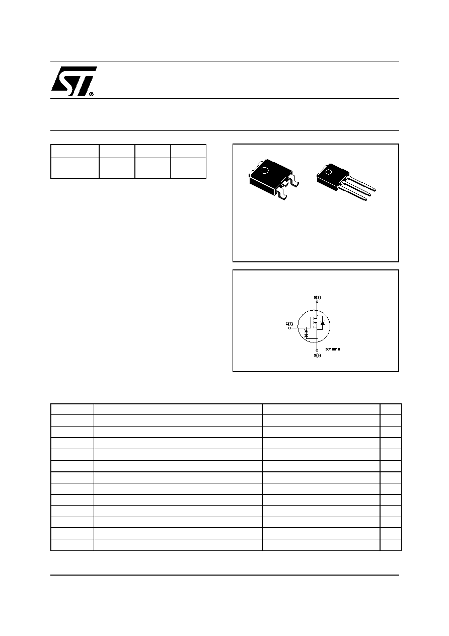
DPAK
TO-252
3
2
1
IPAK
TO-251
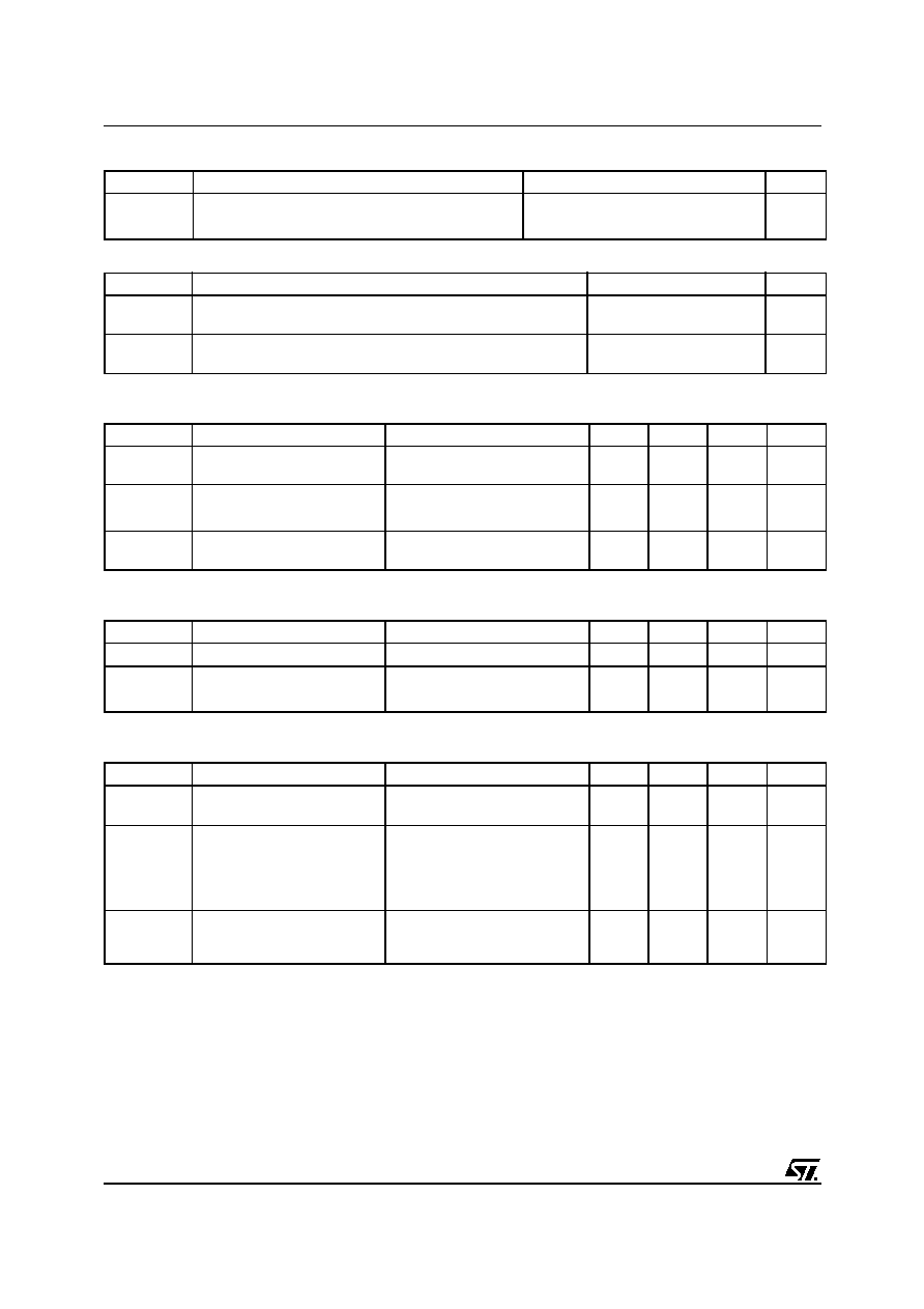
INTERNAL SCHEMATIC DIAGRAM
STD2NM60/STD2NM60-1
2/10
THERMAL DATA
AVALANCHE CHARACTERISTICS
ELECTRICAL CHARACTERISTICS (T
CASE
= 25 ∞C UNLESS OTHERWISE SPECIFIED)
OFF
ON
(1)
DYNAMIC
Note: 1. Pulsed: Pulse duration = 300 µs, duty cycle 1.5 %.
Rthj-case
Thermal Resistance Junction-case Max
2.73
∞C/W
Rthj-amb
Thermal Resistance Junction-ambient Max
62.5
∞C/W
T
l
Maximum Lead Temperature For Soldering Purpose
300
∞C
Symbol
Parameter
Max Value
Unit
I
AR
Avalanche Current, Repetitive or Not-Repetitive
(pulse width limited by T
j
max)
0.5
A
E
AS
Single Pulse Avalanche Energy
(starting T
j
= 25 ∞C, I
D
= I
AR
, V
DD
= 50 V)
250
mJ
Symbol
Parameter
Test Conditions
Min.
Typ.
Max.
Unit
V
(BR)DSS
Drain-source
Breakdown Voltage
I
D
= 1 mA, V
GS
= 0
600
V
I
DSS
Zero Gate Voltage
Drain Current (V
GS
= 0)
V
DS
= Max Rating
1
µA
V
DS
= Max Rating, T
C
= 125 ∞C
10
µA
I
GSS
Gate-body Leakage
Current (V
DS
= 0)
V
GS
= ± 20V
± 5
µA
Symbol
Parameter
Test Conditions
Min.
Typ.
Max.
Unit
V
GS(th)
Gate Threshold Voltage
V
DS
= V
GS
, I
D
= 250µA
3
4
5
V
R
DS(on)
Static Drain-source On
Resistance
V
GS
= 10V, I
D
= 1 A
2.8
3.2
Symbol
Parameter
Test Conditions
Min.
Typ.
Max.
Unit
g
fs
(1)
Forward Transconductance
V
DS
> I
D(on)
x R
DS(on)max,
I
D
= 2 A
1.4
S
C
iss
Input Capacitance
V
DS
= 25V, f = 1 MHz, V
GS
= 0
160
pF
C
oss
Output Capacitance
67
pF
C
rss
Reverse Transfer
Capacitance
4
pF
R
G
Gate Input Resistance
f=1 MHz Gate DC Bias = 0
Test Signal Level = 20mV
Open Drain
3.5
3/10
STD2NM60/STD2NM60-1
ELECTRICAL CHARACTERISTICS (CONTINUED)
SWITCHING ON
SWITCHING OFF
SOURCE DRAIN DIODE
Note: 1. Pulsed: Pulse duration = 300 µs, duty cycle 1.5 %.
2. Pulse width limited by safe operating area.
GATE-SOURCE ZENER DIODE
PROTECTION FEATURES OF GATE-TO-SOURCE ZENER DIODES
The built-in back-to-back Zener diodes have specifically been designed to enhance not only the device's
ESD capability, but also to make them safely absorb possible voltage transients that may occasionally be
applied from gate to source. In this respect the Zener voltage is appropriate to achieve an efficient and
cost-effective intervention to protect the device's integrity. These integrated Zener diodes thus avoid the
usage of external components.
Symbol
Parameter
Test Conditions
Min.
Typ.
Max.
Unit
t
d(on)
t
r
Turn-on Delay Time
Rise Time
V
DD
= 300V, I
D
= 1 A
R
G
= 4.7
V
GS
= 10V
(see test circuit, Figure 3)
13
8
ns
ns
Q
g
Total Gate Charge
V
DD
= 480V, I
D
= 2 A,
V
GS
= 10V
6
8.4
nC
Q
gs
Gate-Source Charge
1.8
nC
Q
gd
Gate-Drain Charge
3.3
nC
Symbol
Parameter
Test Conditions
Min.
Typ.
Max.
Unit
t
r(Voff)
Off-voltage Rise Time
V
DD
= 480 V, I
D
= 2 A,
R
G
= 4.7
,
V
GS
= 10V
(see test circuit, Figure 5)
12
ns
t
f
Fall Time
25
ns
t
c
Cross-over Time
30
ns
Symbol
Parameter
Test Conditions
Min.
Typ.
Max.
Unit
I
SD
Source-drain Current
2
A
I
SDM
(2)
Source-drain Current (pulsed)
8
A
V
SD
(1)
Forward On Voltage
I
SD
= 2 A, V
GS
= 0
1.5
V
t
rr
Q
rr
I
RRM
Reverse Recovery Time
Reverse Recovery Charge
Reverse Recovery Current
I
SD
= 2 A, di/dt = 100A/µs,
V
DD
= 100 V, T
j
= 25∞C
(see test circuit, Figure 5)
516
516
2
ns
nC
A
t
rr
Q
rr
I
RRM
Reverse Recovery Time
Reverse Recovery Charge
Reverse Recovery Current
I
SD
= 2 A, di/dt = 100A/µs,
V
DD
= 100 V, T
j
= 150∞C
(see test circuit, Figure 5)
808
890
2.2
ns
nC
A
Symbol
Parameter
Test Conditions
Min.
Typ.
Max.
Unit
BV
GSO
Gate-Source Breakdown
Voltage
Igs=± 1mA (Open Drain)
30
V
STD2NM60/STD2NM60-1
4/10
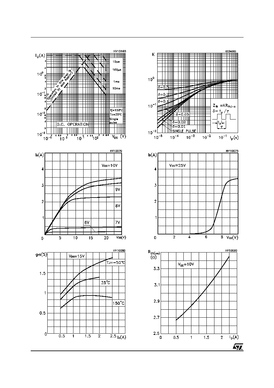
Output Characteristics
Safe Operating Area
Transfer Characteristics
Transconductance
Static Drain-source On Resistance
Thermal Impedance
5/10
STD2NM60/STD2NM60-1
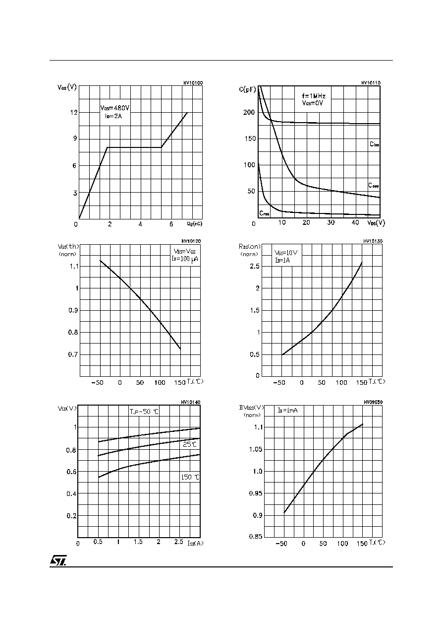
Normalized BVDSS vs. Temperature
Normalized On Resistance vs Temperature
Normalized Gate Thereshold Voltage vs Temp.
Capacitance Variations
Gate Charge vs Gate-source Voltage
Source-drain Diode Forward Characteristics