
1/10
February 2002
.
STD35NF3LL
STD35NF3LL-1
N-CHANNEL 30V - 0.014
- 35A IPAK/DPAK
STripFETTM II POWER MOSFET
s
TYPICAL R
DS
(on) = 0.016
@ 4.5V
s
OPTIMAL R
DS
(on) x Qg TRADE-OFF @ 4.5V
s
CONDUCTION LOSSES REDUCED
s
SWITCHING LOSSES REDUCED
s
LOW THRESHOLD DRIVE
s
THROUGH-HOLE IPAK (TO-251) POWER
PACKAGE IN TUBE (SUFFIX "-1")
s
SURFACE-MOUNTING DPAK (TO-252)
POWER PACKAGE IN TAPE & REEL
(SUFFIX "T4")
DESCRIPTION
This application specific Power MOSFET is the third
genaration of STMicroelectronis unique "Single Feature
SizeTM" strip-based process. The resulting transistor
shows the best trade-off between on-resistance and gate
charge. When used as high and low side in buck
regulators, it gives the best performance in terms of both
conduction and switching losses. This is extremely
important for motherboards where fast switching and
high efficiency are of paramount importance.
APPLICATIONS
s
SPECIFICALLY DESIGNED AND OPTIMISED
FOR HIGH EFFICIENCY DC/DC
CONVERTERS
TYPE
V
DSS
R
DS(on)
I
D
STD35NF3LL
STD35NF3LL-1
30 V
30 V
< 0.0195
< 0.0195
35 A
35 A
3
2
1
1
3
IPAK
TO-251
(Suffix "-1")
DPAK
TO-252
(Suffix "T4")
ABSOLUTE MAXIMUM RATINGS
(
∑)
Pulse width limited by safe operating area.
(1) Starting T
j
= 25
o
C, I
D
= 17.5 A, V
DD
= 24 V
Symbol
Parameter
Value
Unit
V
DS
Drain-source Voltage (V
GS
= 0)
30
V
V
DGR
Drain-gate Voltage (R
GS
= 20 k
)
30
V
V
GS
Gate- source Voltage
± 16
V
I
D
Drain Current (continuos) at T
C
= 25∞C
35
A
I
D
Drain Current (continuos) at T
C
= 100∞C
25
A
I
DM
(
∑)
Drain Current (pulsed)
140
A
P
tot
Total Dissipation at T
C
= 25∞C
50
W
Derating Factor
0.33
W/∞C
E
AS (1)
Single Pulse Avalanche Energy
300
mJ
T
stg
Storage Temperature
-55 to 175
∞C
T
j
Max. Operating Junction Temperature
INTERNAL SCHEMATIC DIAGRAM
STD35NF3LL/STD35NF3LL-1
2/10
THERMAL DATA
ELECTRICAL CHARACTERISTICS (T
case
= 25 ∞C unless otherwise specified)
OFF
ON
(*)
DYNAMIC
Rthj-case
Rthj-amb
T
l
Thermal Resistance Junction-case
Thermal Resistance Junction-ambient
Maximum Lead Temperature For Soldering Purpose
Max
Max
Typ
3
100
300
∞C/W
∞C/W
∞C
Symbol
Parameter
Test Conditions
Min.
Typ.
Max.
Unit
V
(BR)DSS
Drain-source
Breakdown Voltage
I
D
= 250 µA, V
GS
= 0
30
V
I
DSS
Zero Gate Voltage
Drain Current (V
GS
= 0)
V
DS
= Max Rating
V
DS
= Max Rating T
C
= 100∞C
1
10
µA
µA
I
GSS
Gate-body Leakage
Current (V
DS
= 0)
V
GS
= ± 16 V
±100
nA
Symbol
Parameter
Test Conditions
Min.
Typ.
Max.
Unit
V
GS(th)
Gate Threshold Voltage
V
DS
= V
GS
I
D
= 250 µA
1
V
R
DS(on)
Static Drain-source On
Resistance
V
GS
= 10 V
I
D
= 17.5 A
V
GS
= 4.5 V
I
D
= 17.5 A
0.014
0.016
0.0195
0.0215
Symbol
Parameter
Test Conditions
Min.
Typ.
Max.
Unit
g
fs (*)
Forward Transconductance
V
DS
=15 V
I
D
= 17.5 A
19
S
C
iss
C
oss
C
rss
Input Capacitance
Output Capacitance
Reverse Transfer
Capacitance
V
DS
= 25V, f = 1 MHz, V
GS
= 0
800
250
60
pF
pF
pF
3/10
STD35NF3LL/STD35NF3LL-1
SWITCHING ON
SWITCHING OFF
SOURCE DRAIN DIODE
(*)
Pulsed: Pulse duration = 300 µs, duty cycle 1.5 %.
(
∑)
Pulse width limited by safe operating area.
Symbol
Parameter
Test Conditions
Min.
Typ.
Max.
Unit
t
d(on)
t
r
Turn-on Delay Time
Rise Time
V
DD
= 15 V
I
D
= 17.5 A
R
G
= 4.7
V
GS
= 4.5 V
(Resistive Load, Figure 3)
17
100
ns
ns
Q
g
Q
gs
Q
gd
Total Gate Charge
Gate-Source Charge
Gate-Drain Charge
V
DD
= 24 V I
D
= 35 A V
GS
= 5V
12.5
4.2
5.2
17
nC
nC
nC
Symbol
Parameter
Test Conditions
Min.
Typ.
Max.
Unit
t
d(off)
t
f
Turn-off Delay Time
Fall Time
V
DD
= 15 V
I
D
= 17.5 A
R
G
= 4.7
V
GS
= 4.5 V
(Resistive Load, Figure 3)
20
21
ns
ns
Symbol
Parameter
Test Conditions
Min.
Typ.
Max.
Unit
I
SD
I
SDM
(
∑
)
Source-drain Current
Source-drain Current (pulsed)
35
140
A
A
V
SD
(*)
Forward On Voltage
I
SD
= 35 A
V
GS
= 0
1.3
V
t
rr
Q
rr
I
RRM
Reverse Recovery Time
Reverse Recovery Charge
Reverse Recovery Current
I
SD
= 35 A
di/dt = 100A/µs
V
DD
= 15 V
T
j
= 150∞C
(see test circuit, Figure 5)
35
44
2.5
ns
nC
A
ELECTRICAL CHARACTERISTICS (continued)
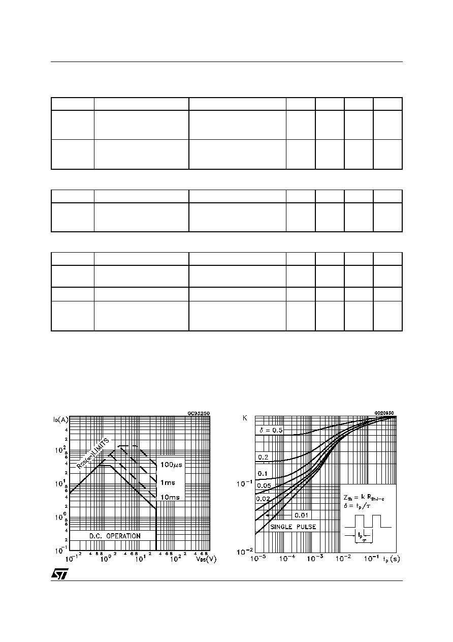
Safe Operating Area
Thermal Impedance
STD35NF3LL/STD35NF3LL-1
4/10
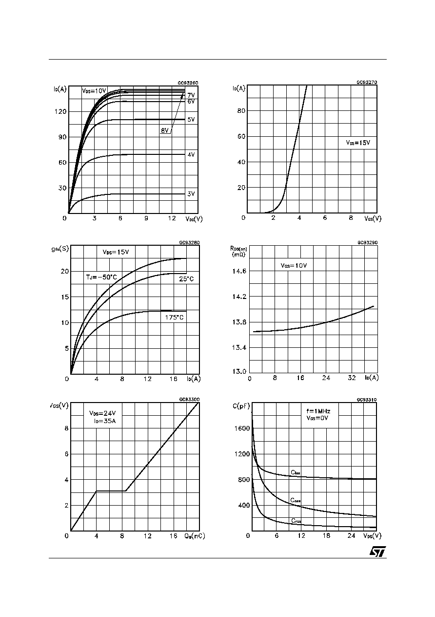
Output Characteristics
Transfer Characteristics
Transconductance
Static Drain-source On Resistance
Gate Charge vs Gate-source Voltage
Capacitance Variations
5/10
STD35NF3LL/STD35NF3LL-1
.
.
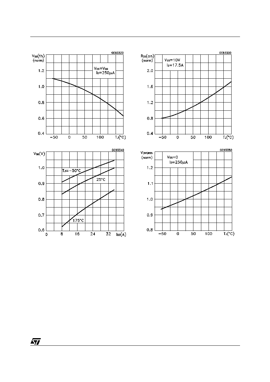
Normalized Gate Threshold Voltage vs Temperature
Normalized on Resistance vs Temperature
Source-drain Diode Forward Characteristics
Normalized Breakdown Voltage vs Temperature.
.
.