1/10
June 2003
STD3PS25 - STD3PS25-1
P-CHANNEL 250V - 2.1
- 3A DPAK/IPAK
MESH OVERLAYTM MOSFET
s
TYPICAL R
DS
(on) = 2.1
s
100% AVALANCHE TESTED
s
APPLICATION ORIENTED
CHARACTERIZATION
s
STANDARD OUTLINE FOR EASY
AUTOMATED SURFACE MOUNT ASSEMBLY
s
GATE-SOURCE ZENER DIODE
DESCRIPTION
Using the latest high voltage MESH OVERLAYTM
process, STMicroelectronics has designed an ad-
vanced family of power MOSFETs with outstanding
performance. The new patented STrip layout cou-
pled with the Company's proprietary edge termina-
tion structure, makes it suitable in coverters for
lighting applications.
APPLICATIONS
s
CONSUMER
s
LIGHTING
ABSOLUTE MAXIMUM RATINGS
TYPE
V
DSS
R
DS(on)
I
D
STD3PS25
STD3PS25-1
250 V
250 V
< 2.8
< 2.8
3 A
3 A
Symbol
Parameter
Value
Unit
V
DS
Drain-source Voltage (V
GS
= 0)
250
V
V
DGR
Drain-gate Voltage (R
GS
= 20 k
)
250
V
V
GS
Gate- source Voltage
±25
V
I
D
Drain Current (continuous) at T
C
= 25∞C
3
A
I
D
Drain Current (continuous) at T
C
= 100∞C
1.9
A
I
DM
(1)
Drain Current (pulsed)
12
A
P
TOT
Total Dissipation at T
C
= 25∞C
45
W
Derating Factor
0.36
W/∞C
T
stg
Storage Temperature
≠ 50 to 150
∞C
T
j
Max. Operating Junction Temperature
150
∞C
DPAK
1
3
IPAK
3
2
1
INTERNAL SCHEMATIC DIAGRAM
STD3PS25 - STD3PS25-1
2/10
THERMAL DATA
ELECTRICAL CHARACTERISTICS (T
CASE
= 25 ∞C UNLESS OTHERWISE SPECIFIED)
OFF
ON
DYNAMIC
Rthj-case
Thermal Resistance Junction-case Max
2.77
∞C/W
Rthj-amb
Thermal Resistance Junction-ambient Max
100
∞C/W
T
l
Maximum Lead Temperature For Soldering Purpose
275
∞C
Symbol
Parameter
Test Conditions
Min.
Typ.
Max.
Unit
V
(BR)DSS
Drain-source
Breakdown Voltage
I
D
= 250 µA, V
GS
= 0
250
V
I
DSS
Zero Gate Voltage
Drain Current (V
GS
= 0)
V
DS
= Max Rating
1
µA
V
DS
= Max Rating, T
C
= 125 ∞C
10
µA
I
GSS
Gate-body Leakage
Current (V
DS
= 0)
V
GS
= ± 20 V
±10
µA
Symbol
Parameter
Test Conditions
Min.
Typ.
Max.
Unit
V
GS(th)
Gate Threshold Voltage
V
DS
= V
GS
, I
D
= 250 µA
2
3
4
V
R
DS(on)
Static Drain-source On
Resistance
V
GS
= 10 V, I
D
= 0.3 A
2.1
2.8
Symbol
Parameter
Test Conditions
Min.
Typ.
Max.
Unit
C
iss
Input Capacitance
V
DS
= 25 V, f = 1 MHz, V
GS
= 0
260
pF
C
oss
Output Capacitance
52
pF
C
rss
Reverse Transfer
Capacitance
25
pF
R
G
Gate-Input Resistance
f = 1 MHz,Gate DC Bias=0
Test Signal Level=20 mV
Open Drain
6
3/10
STD3PS25 - STD3PS25-1
ELECTRICAL CHARACTERISTICS (CONTINUED)
SWITCHING ON
SWITCHING OFF
SOURCE DRAIN DIODE
GATE-SOURCE ZENER DIODE
(4) Pulsed: Pulse duration = 300 µs, duty cycle 1.5 %.
(5) Pulse width limited by safe operating area
PROTECTION FEATURES OF GATE-TO-SOURCE ZENER DIODES
The built-in back-to-back Zener diodes have specifically been designed to enhance not only the device's
ESD capability, but also to make them safely absorb possible voltage transients that may occasionally be
applied from gate to source. In this respect the Zener voltage is appropriate to achieve an efficient and
cost-effective intervention to protect the device's integrity. These integrated Zener diodes thus avoid the
usage of external components.
Symbol
Parameter
Test Conditions
Min.
Typ.
Max.
Unit
t
d(on)
t
r
Turn-on Delay Time
Rise Time
V
DD
= 125V, I
D
= 1.5A
R
G
= 4.7
V
GS
= 10V
(Resistive, see Figure 3)
12
22
ns
ns
Q
g
Q
gs
Q
gd
Total Gate Charge
Gate-Source Charge
Gate-Drain Charge
V
DD
= 200V, I
D
= 1.5A,
V
GS
= 10V
16
1.4
7.6
21
nC
nC
nC
Symbol
Parameter
Test Conditions
Min.
Typ.
Max.
Unit
t
d(off)
t
f
Turn-off Delay Time
Fall Time
V
DD
= 200V, I
D
= 1.5A,
R
G
= 4.7
,
V
GS
= 10V
(see test circuit, Figure 5)
29.5
7
ns
ns
Symbol
Parameter
Test Conditions
Min.
Typ.
Max.
Unit
I
SD
I
SDM
(4)
Source-drain Current
Source-drain Current (pulsed)
3
12
A
A
V
SD
(5)
Forward On Voltage
I
SD
= 3A, V
GS
= 0
1.5
V
t
rr
Q
rr
I
RRM
Reverse Recovery Time
Reverse Recovery Charge
Reverse Recovery Curren
I
SD
= 0.60A, di/dt = 100A/µs,
V
DD
= 40V, T
j
= 150∞C
(see test circuit, Figure 5)
143
806
11
ns
nC
A
Symbol
Parameter
Test Conditions
Min.
Typ.
Max.
Unit
BV
GSO
Gate-Source Breakdown
Voltage
Igs=± 500 µA (Open Drain)
± 25
V
STD3PS25 - STD3PS25-1
4/10
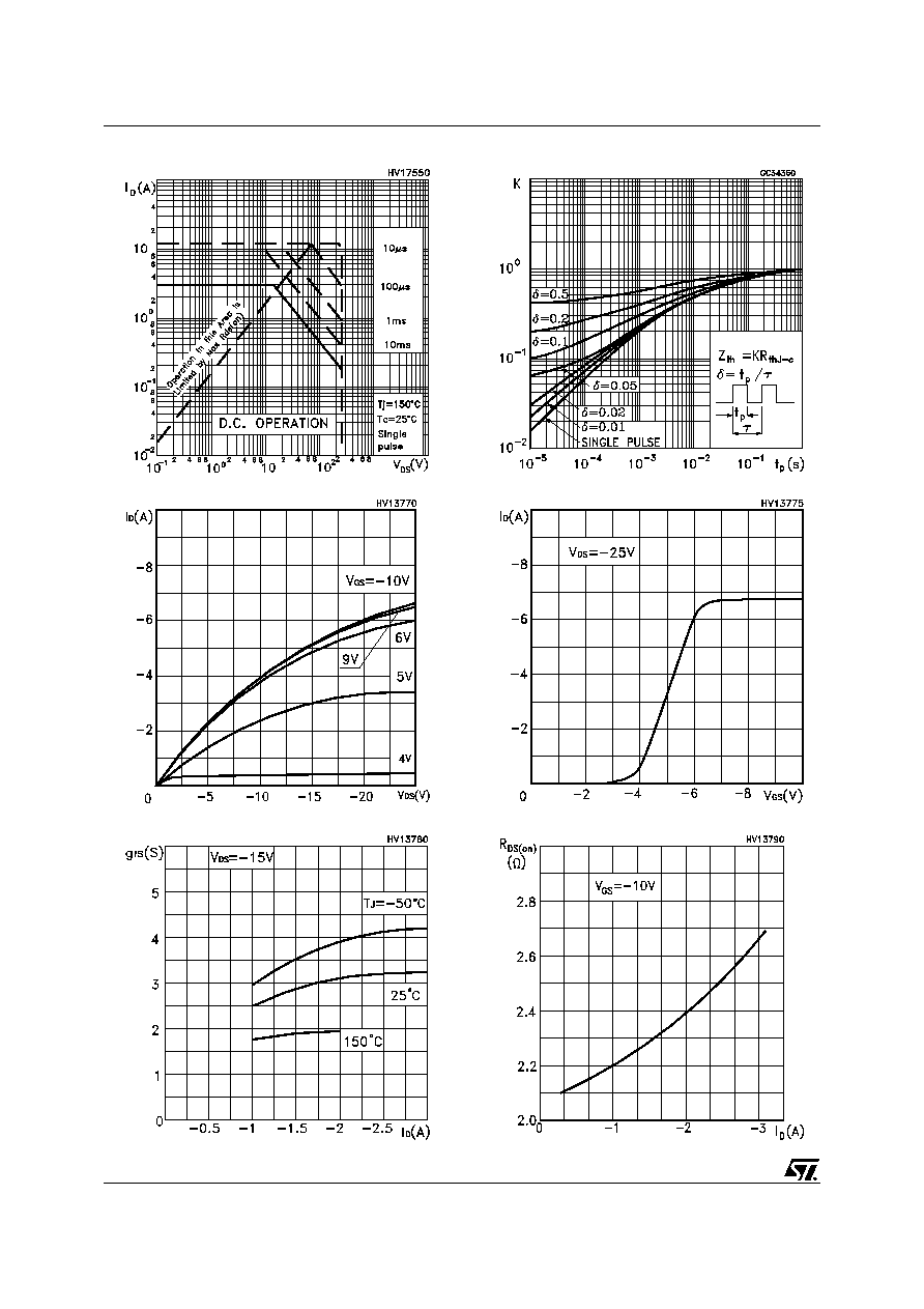
Safe Operating Area p-ch
Output Characteristics p-ch
Transfer Characteristics p-ch
Static Drain-source On Resistance p-ch
Transconductance p-ch
Thermal Impedance for Complementary pair
5/10
STD3PS25 - STD3PS25-1
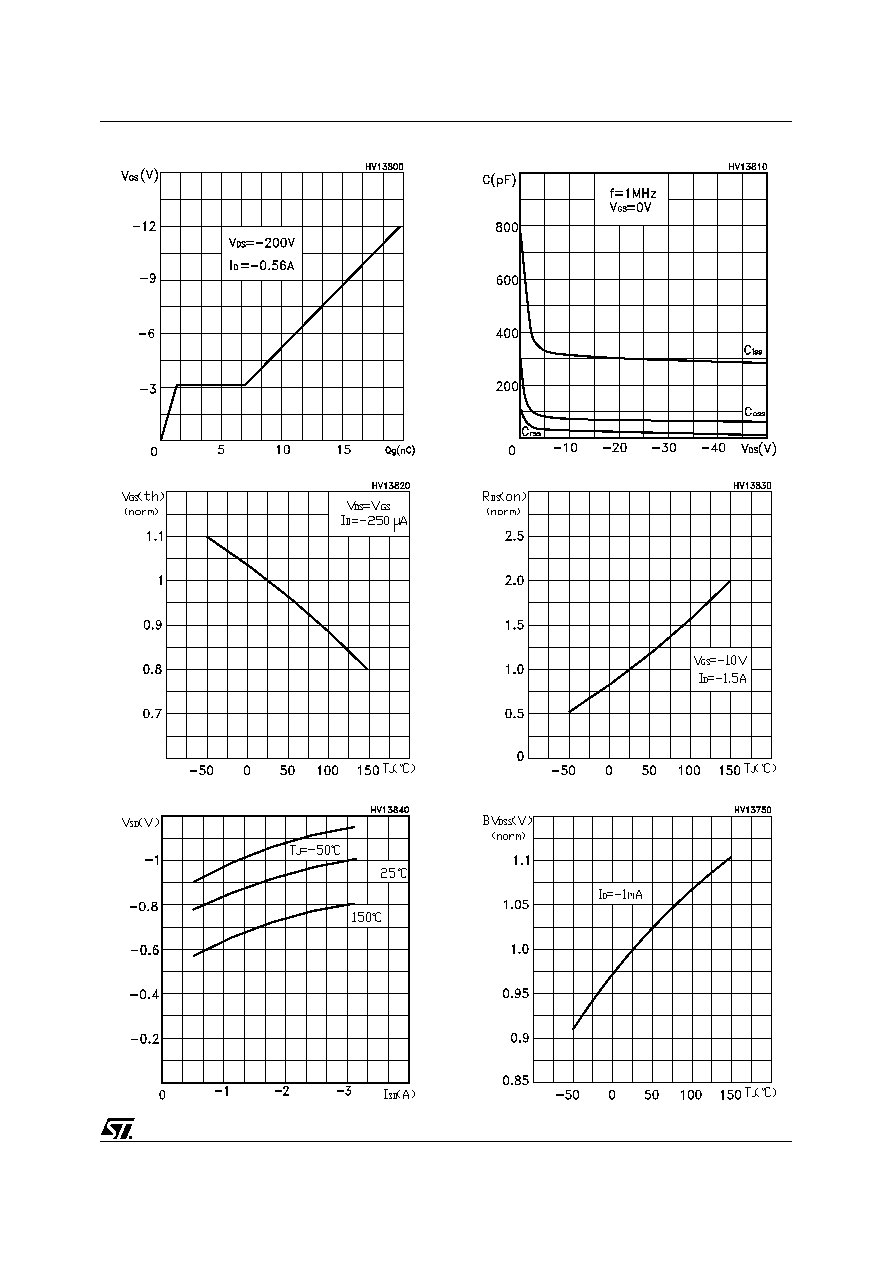
NormalizedOnResistancevsTemperaturep-ch
Norm. Gate Thereshold Voltage vs Temp p-ch
Source-drainDiodeForwardCharacteristicsp-ch
Capacitance Variations p-ch
Gate Charge vs Gate-source Voltage p-ch
Normalized BVDSS vs Temperature p-ch