STD40NF03L
N-CHANNEL 30V - 0.012
- 40A DPAK
LOW GATE CHARGE STripFET
TM
POWER MOSFET
PRELIMINARY DATA
s
TYPICAL R
DS(on)
= 0.012
s
TYPICAL Q
g
= 35 nC @ 10V
s
OPTIMAL R
DS(on)
x Q
g
TRADE-OFF
s
CONDUCTION LOSSES REDUCED
s
SWITCHING LOSSES REDUCED
DESCRIPTION
This application specific Power Mosfet is the third
generation of STMicroelectronics unique "Single
Feature Size
TM
" strip-based process. The resul-
ting transistor shows the best trade-off between
on-resistance and gate charge. When used as
high and low side in buck regulators, it gives the
best performance in terms of both conduction and
switching losses. This is extremely important for
motherboards where fast switching and high effi-
ciency are of paramount importance.
APPLICATIONS
s
SPECIFICALLY DESIGNED AND
OPTIMISED FOR HIGH EFFICIENCY CPU
CORE DC/DC CONVERTERS
�
INTERNAL SCHEMATIC DIAGRAM
14/01/2000
ABSOLUTE MAXIMUM RATINGS
Symbol
Parameter
Value
Un it
V
DS
Drain-source Voltage (V
GS
= 0)
30
V
V
DGR
Drain- gate Voltage (R
GS
= 20 k
)
30
V
V
GS
G ate-source Volt age
�
20
V
I
D
(
�)
Drain Current (continuous) at T
c
= 25
o
C
20
A
I
D
Drain Current (continuous) at T
c
= 100
o
C
20
A
I
DM
(
��)
Drain Current (pulsed)
80
A
P
tot
T otal Dissipat ion at T
c
= 25
o
C
55
W
Derating Factor
0.37
W /
o
C
T
s tg
Storage Temperature
-65 to 175
o
C
T
j
Max. Operating Junction Temperature
175
o
C
(
�)
Current Limited By The Package
(
��)
Pulse width limited by safe operating area
T YPE
V
DSS
R
DS(on)
I
D
STD40NF03L
30 V
< 0.014
40 A
ADD SUFFIX "T4" FOR ORDERING IN TAPE & REEL
1
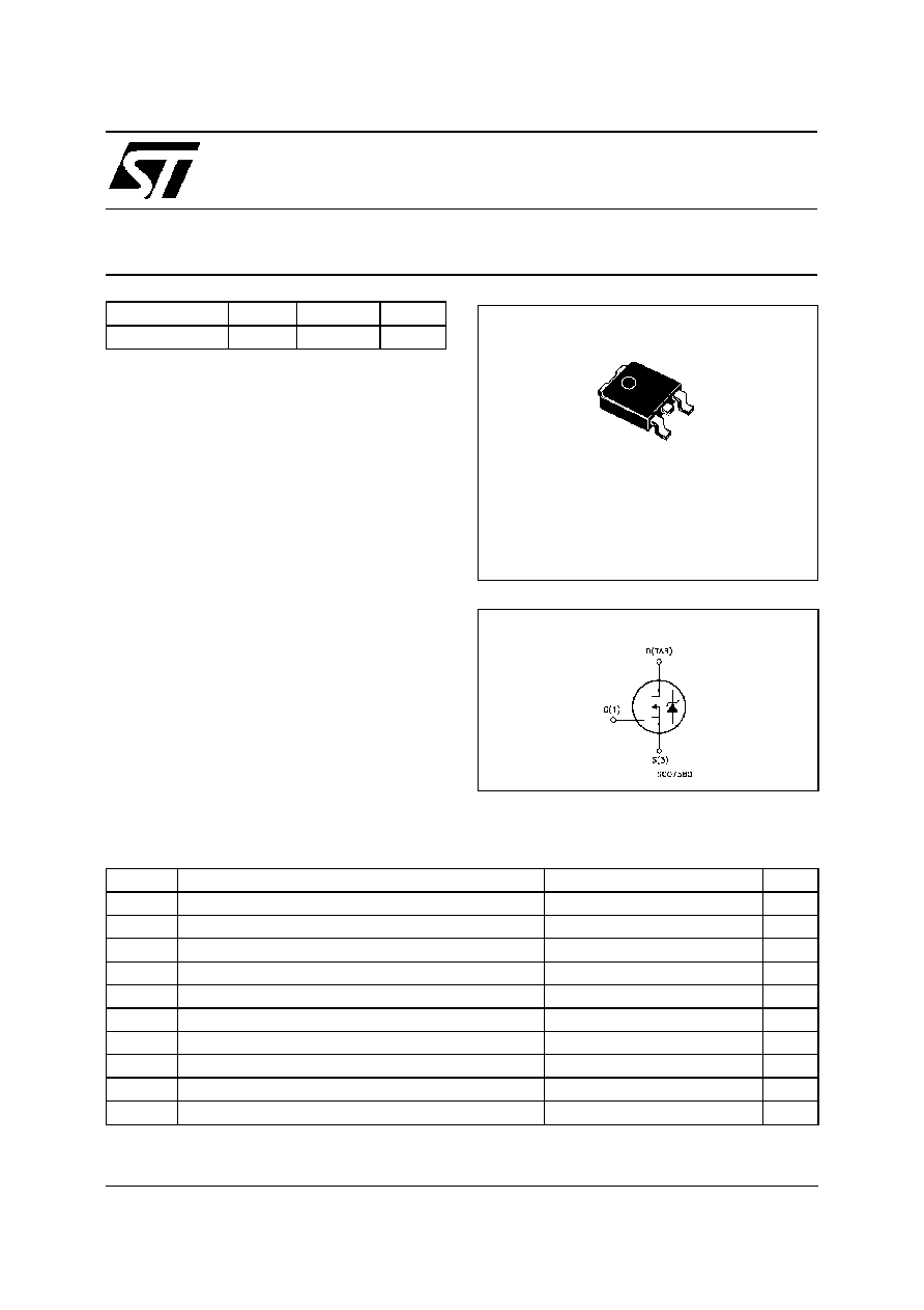
3
DPAK
TO-252
(Suffix "T4")
1/6
THERMAL DATA
R
thj -case
R
thj -amb
T
l
Thermal Resistance Junction-case
Max
Thermal Resistance Junction-ambient
Max
Maximum Lead Temperature F or Soldering Purpose
2.73
62.5
300
o
C/W
o
C/W
o
C
ELECTRICAL CHARACTERISTICS (T
case
= 25
o
C unless otherwise specified)
OFF
Symbo l
Parameter
Test Con ditions
Min.
Typ.
Max.
Unit
V
(BR)DSS
Drain-source
Breakdown Voltage
I
D
= 250
�
A
V
GS
= 0
30
V
I
DSS
Zero Gat e Voltage
Drain Current (V
GS
= 0)
V
DS
= Max Rat ing
V
DS
= Max Rat ing
T
c
=125
o
C
1
10
�
A
�
A
I
G SS
Gat e-body Leakage
Current (V
DS
= 0)
V
GS
=
�
20 V
�
100
nA
ON (
)
Symbo l
Parameter
Test Con ditions
Min.
Typ.
Max.
Unit
V
G S(th)
Gat e Threshold Voltage V
DS
= V
GS
I
D
= 250
�
A
1
2. 5
V
R
DS(on)
Static Drain-source On
Resistance
V
GS
= 10V
I
D
= 20 A
V
GS
= 5V
I
D
= 20 A
0.012
0.019
0.014
0.022
I
D(o n)
On State Drain Current
V
DS
> I
D(o n)
x R
DS(on )ma x
V
GS
= 10 V
40
A
DYNAMIC
Symbo l
Parameter
Test Con ditions
Min.
Typ.
Max.
Unit
g
f s
(
)
Forward
Transconductance
V
DS
> I
D(o n)
x R
DS(on )ma x
I
D
=20 A
40
S
C
iss
C
os s
C
rss
Input Capacitance
Out put Capacitance
Reverse Transfer
Capacitance
V
DS
= 25 V
f = 1 MHz
V
GS
= 0
1470
490
110
pF
pF
pF
STD40NF03L
2/6
ELECTRICAL CHARACTERISTICS (continued)
SWITCHING ON
Symbo l
Parameter
Test Con ditions
Min.
Typ.
Max.
Unit
t
d(on)
t
r
Turn-on Delay T ime
Rise Time
V
DD
= 15 V
I
D
= 20 A
R
G
= 4.7
V
G S
= 4.5 V
(Resistive Load, see fig. 3)
20
170
ns
ns
Q
g
Q
gs
Q
gd
Tot al G ate Charge
Gat e-Source Charge
Gat e-Drain Charge
V
DD
= 24 V I
D
= 40 A V
GS
= 10 V
35
5
10
45
nC
nC
nC
SWITCHING OFF
Symbo l
Parameter
Test Con ditions
Min.
Typ.
Max.
Unit
t
d(of f)
t
f
Turn-off Delay T ime
Fall T ime
V
DD
= 15 V
I
D
= 20 A
R
G
= 4.7
V
G S
= 4.5 V
(Resistive Load, see fig. 3)
40
60
ns
ns
SOURCE DRAIN DIODE
Symbo l
Parameter
Test Con ditions
Min.
Typ.
Max.
Unit
I
SD
I
SDM
(
�
)
Source-drain Current
Source-drain Current
(pulsed)
20
80
A
A
V
SD
(
)
Forward On Voltage
I
SD
=20 A
V
GS
= 0
1. 5
V
t
rr
Q
rr
I
RRM
Reverse Recovery
Time
Reverse Recovery
Charge
Reverse Recovery
Current
I
SD
= 20 A
di/dt = 100 A/
�
s
V
DD
= 15 V
T
j
= 150
o
C
(see t est circuit, f ig. 5)
70
105
2.4
ns
nC
A
(
) Pulsed: Pulse duration = 300
�
s, duty cycle 1.5 %
(
�
) Pulse width limited by safe operating area
STD40NF03L
3/6
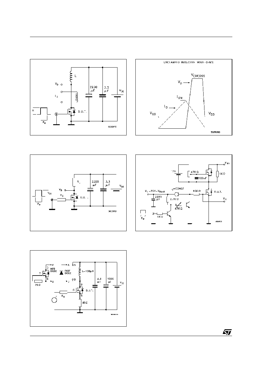
Fig. 1: Unclamped Inductive Load Test Circuit
Fig. 3: Switching Times Test Circuits For
Resistive Load
Fig. 2: Unclamped Inductive Waveform
Fig. 4: Gate Charge test Circuit
Fig. 5: Test Circuit For Inductive Load Switching
And Diode Recovery Times
STD40NF03L
4/6
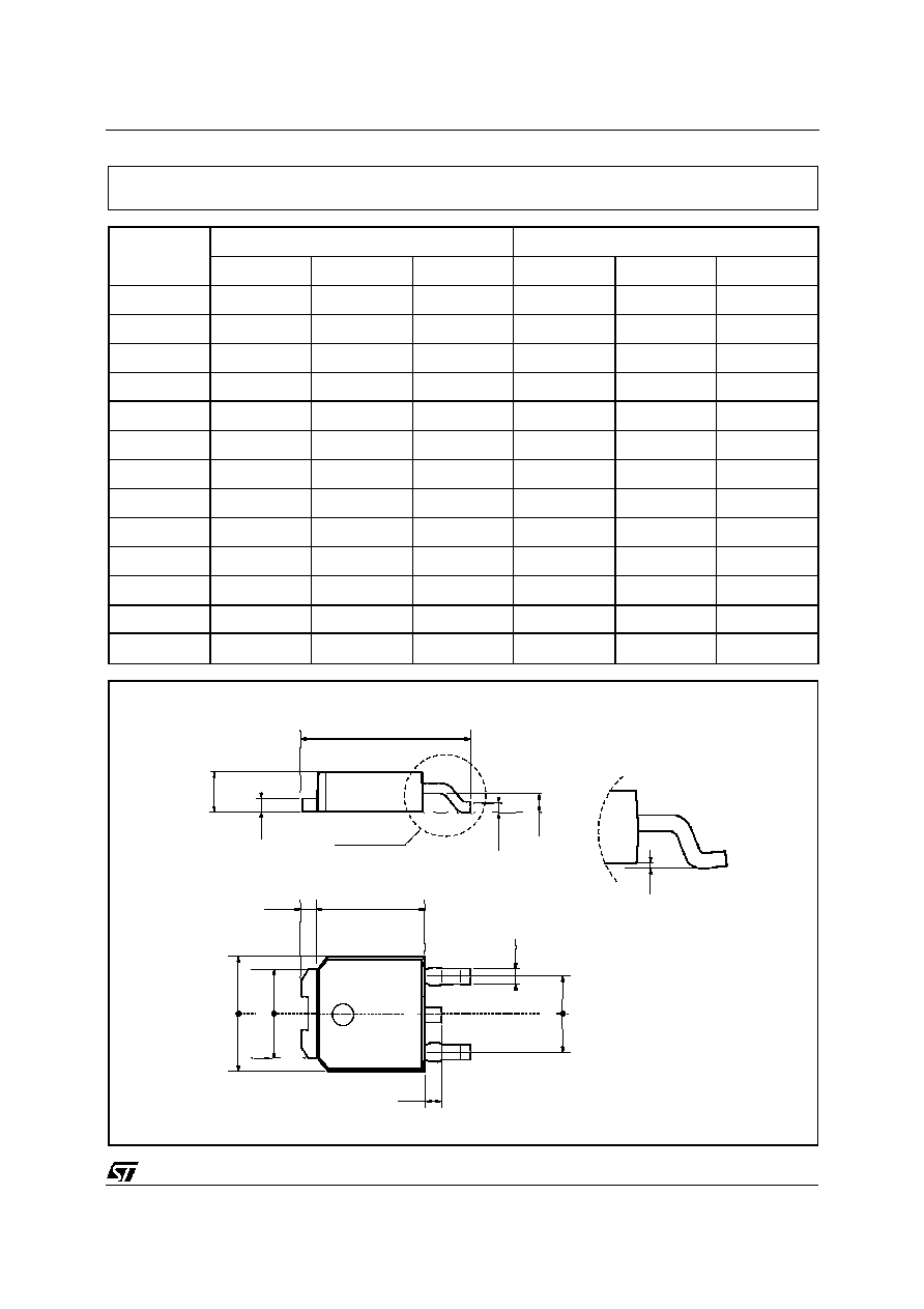
DIM.
mm
inch
MIN.
TYP.
MAX.
MIN.
TYP.
MAX.
A
2.2
2.4
0.086
0.094
A1
0.9
1.1
0.035
0.043
A2
0.03
0.23
0.001
0.009
B
0.64
0.9
0.025
0.035
B2
5.2
5.4
0.204
0.212
C
0.45
0.6
0.017
0.023
C2
0.48
0.6
0.019
0.023
D
6
6.2
0.236
0.244
E
6.4
6.6
0.252
0.260
G
4.4
4.6
0.173
0.181
H
9.35
10.1
0.368
0.397
L2
0.8
0.031
L4
0.6
1
0.023
0.039
==
D
L2
L4
13
==
B
E
==
B2
G
2
A
C2
C
H
A1
DETAIL "A"
A2
DETAIL "A"
TO-252 (DPAK) MECHANICAL DATA
0068772-B
STD40NF03L
5/6