Rev 2
October 2005
1/10
10
STD724
NPN MEDIUM POWER TRANSISTORS
Features
SURFACE MOUNTING DEVICE IN MEDIUM
POWER DPAK POWER PACKAGE
AVAILABLE IN TAPE & REEL PACKING
IN COMPLIANCE WITH THE 2002/93/EC
EUROPEAN DIRECTIVE
Applications
VOLTAGE REGULATION
RELAY DRIVER
GENERIC SWITCH
Description
The device is a NPN transistor manufactured
using planar Technology resulting in rugged high
performance devices.
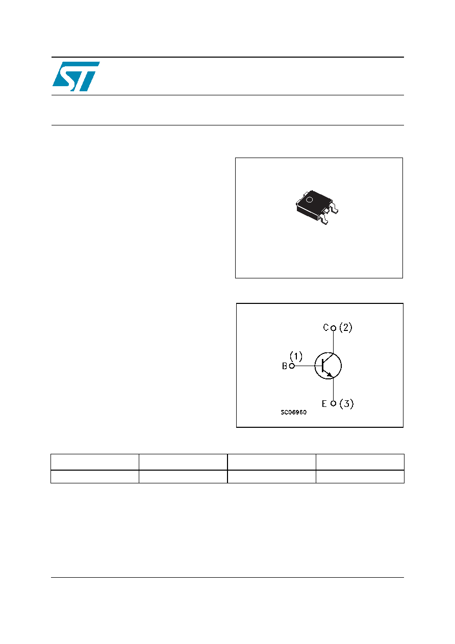
Order codes
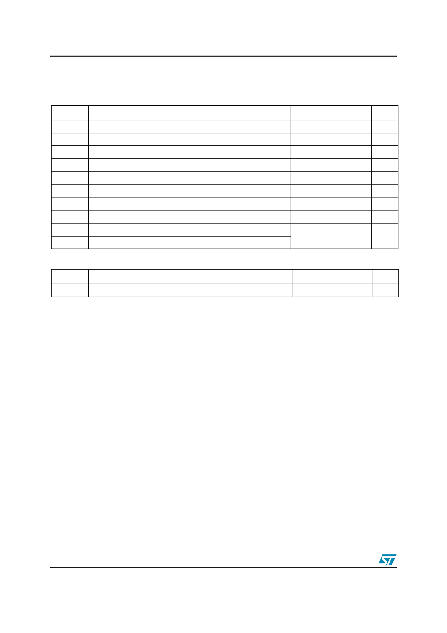
Internal Schematic Diagram
1
3
DPAK
Part Number
Marking
Package
Packing
STD724T4
D724
DPAK
Tape & reel
www.st.com
1 Electrical Ratings
STD724
2/10
1 Electrical
Ratings
Table 1.
Absolute Maximum Rating
Table 2.
Thermal Data
Symbol
Parameter
Value
Unit
V
CBO
Collector-Base Voltage (I
E
= 0)
60
V
V
CEO
Collector-Emitter Voltage (I
B
= 0)
30
V
V
EBO
Collector-Base Voltage (I
C
= 0)
5
V
I
C
Collector Current
3
A
I
CM
Collector Peak Current (t
P
< 5ms)
6
A
I
B
Base Current
1
A
I
BM
Base Peak Current (t
P
< 5ms)
2
A
P
TOT
Total dissipation at T
c
= 25�C
15
W
T
STG
Storage Temperature
-65 to 150
150
�C
T
J
Max. Operating Junction Temperature
Symbol
Parameter
Value
Unit
R
thj-amb
Thermal Resistance Junction-Amb
____________________
Max
8.33
�C/W
STD724
2 Electrical Characteristics
3/10
2 Electrical
Characteristics
Table 3.
Electrical Characteristics (T
CASE
= 25�C; unless otherwise specified)
1 Pulsed duration = 300
s, duty cycle
1.5%.
Symbol
Parameter
Test Conditions
Min.
Typ.
Max.
Unit
I
CES
Collector Cut-off Current
(V
BE
= 0)
V
CE
= 60V
10
A
I
CEO
Collector Cut-off Current
(I
B
= 0)
V
CE
= 30V
100
A
I
EBO
Emitter Cut-off Current
(I
C
= 0)
V
EB
= 5V
10
A
V
(BR)CBO
Collector-Base
Breakdown Voltage (I
E
= 0)
I
C
= 100
A
60
V
V
(BR)CEO
Note 1
Collector-Emitter Breakdown
Voltage (I
B
= 0)
I
C
= 10 mA
30
V
V
(BR)EBO
Collector-Emitter Breakdown
Voltage (I
C
= 0)
I
E
= 100
A
5
V
V
CE(sat)
Note 1
Collector-Emitter Saturation
Voltage
I
C
= 1 A I
B
= 50 mA
I
C
= 2 A I
B
= 100 mA
I
C
= 3 A I
B
= 150 mA
0.4
0.7
1.1
V
V
V
V
BE(sat)
Note 1
Base-Emitter Saturation Voltage I
C
= 2 A I
B
= 100 mA
1.2
V
h
FE
DC Current Gain
I
C
= 100 mA V
CE
= 2 V
I
C
= 1 A V
CE
= 2 V
I
C
= 3 A V
CE
= 2 V
100
80
30
300
f
T
Transistor Frequency
V
CE
= 10 V I
c
= 0.1 A
100
MHz
2 Electrical Characteristics
STD724
4/10
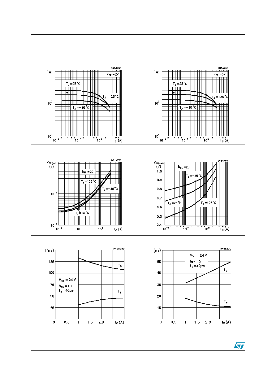
2.1 Electrical
characteristics
(curve)
Figure 1.
DC Current Gain
Figure 2.
DC Current Gain
Figure 3.
Collector-emitter saturation voltage Figure 4.
Base-emitter saturation voltage
Figure 5.
Switching times on resistive load
Figure 6.
Switching times resistive on load
STD724
2 Electrical Characteristics
5/10
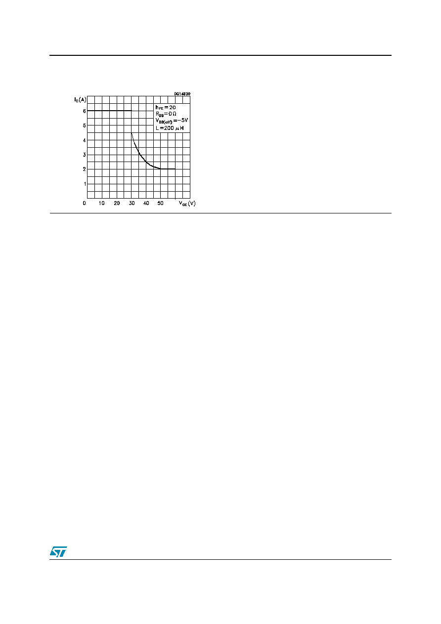
Figure 7.
Reverse biased area