 | –≠–ª–µ–∫—Ç—Ä–æ–Ω–Ω—ã–π –∫–æ–º–ø–æ–Ω–µ–Ω—Ç: STD90N03L | –°–∫–∞—á–∞—Ç—å:  PDF PDF  ZIP ZIP |
October 2006
Rev1
1/16
16
R
DS(on)
*Q
g
industry's benchmark
Conduction losses reduced
Switching losses reduced
Low threshold device
Description
This device utilizes the latest advanced design
rules of ST's proprietary STripFETTM technology.
This is suitable for the most demanding DC-DC
converter application where high efficiency is to
be achieved.
Applications
Switching applications
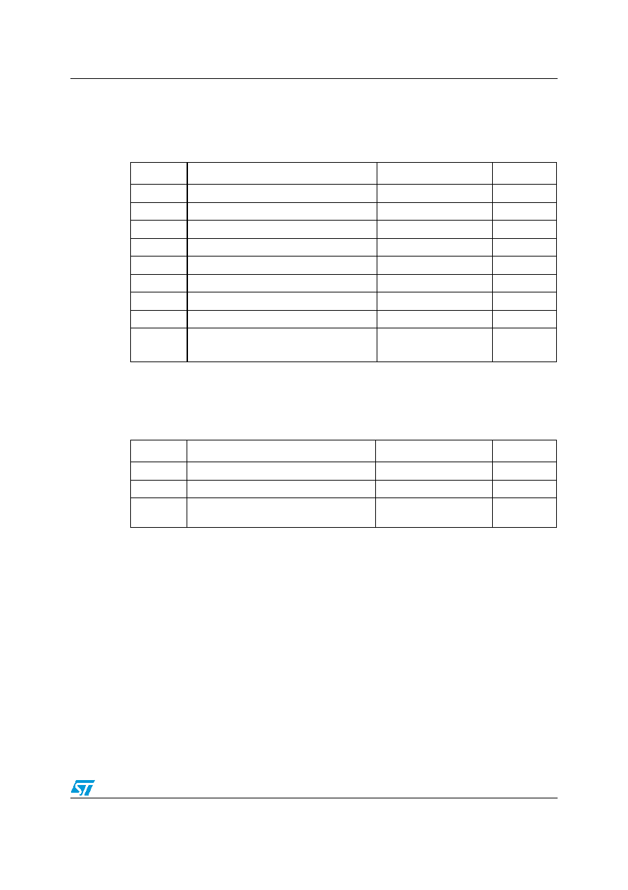
Internal schematic diagram
General features
Type
V
DSS
R
DS(on)
I
D
STD90N03L
STD90N03L-1
30V
30V
0.0057
0.0057
80A
(1)
80A
(1)
1.
Pulse width limited by safe operating area
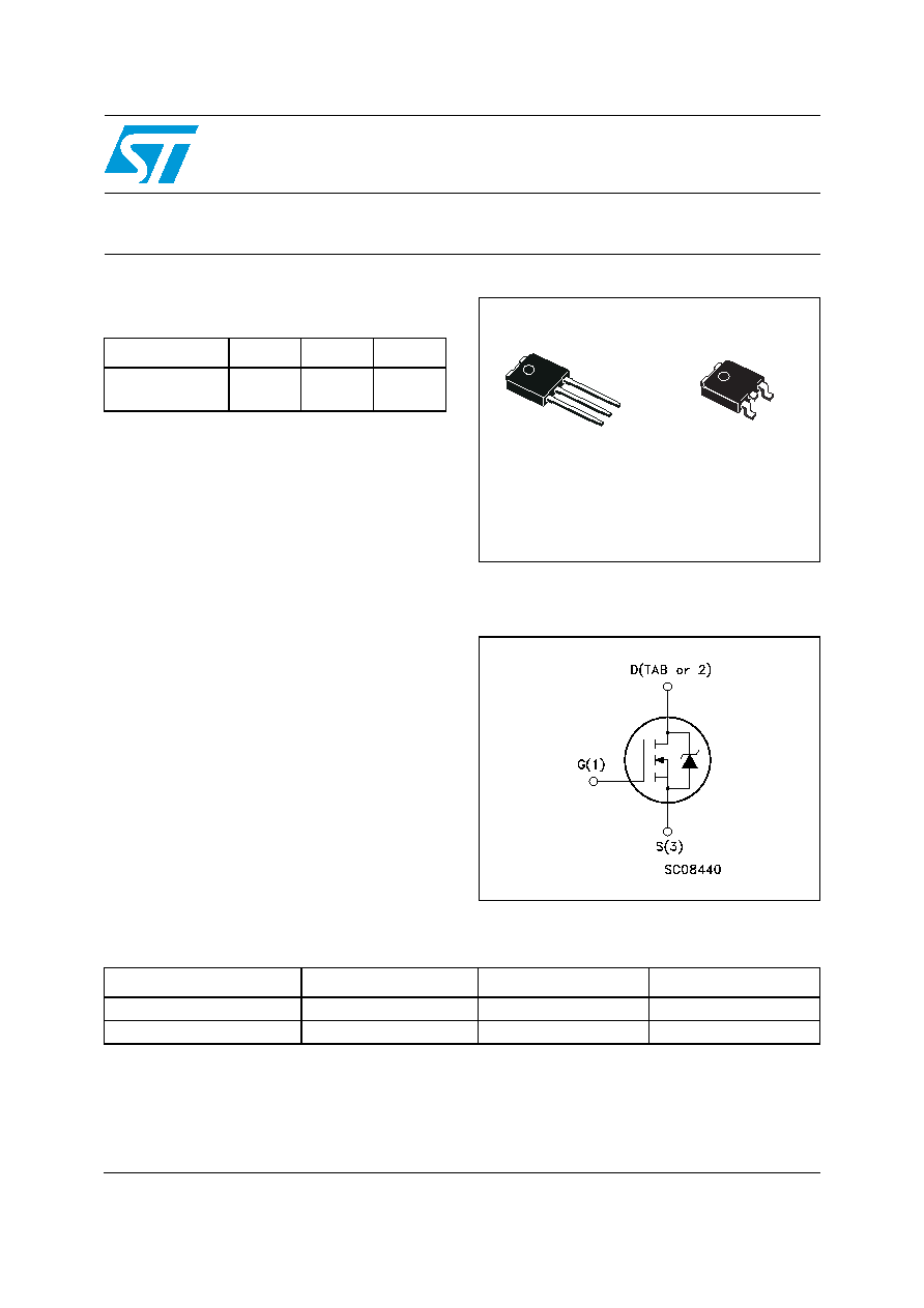
IPAK
3
2
1
1
3
DPAK
STD90N03L
STD90N03L-1
N-channel 30V - 0.005
- 80A - DPAK/IPAK
STripFETTM III Power MOSFET
www.st.com
Order codes
Part number
Marking
Package
Packaging
STD90N03L
D90N03L
DPAK
Tape & reel
STD90N03L-1
D90N03L-1
IPAK
Tube

Content
STD90N03L - STD90N03L-1
2/16
Content
1
Electrical ratings . . . . . . . . . . . . . . . . . . . . . . . . . . . . . . . . . . . . . . . . . . . . 3
2
Electrical characteristics . . . . . . . . . . . . . . . . . . . . . . . . . . . . . . . . . . . . . 4
2.1
Electrical characteristics (curves) . . . . . . . . . . . . . . . . . . . . . . . . . . . . . 6
3
Test circuit . . . . . . . . . . . . . . . . . . . . . . . . . . . . . . . . . . . . . . . . . . . . . . . . 8
4
Package mechanical data . . . . . . . . . . . . . . . . . . . . . . . . . . . . . . . . . . . . 11
5
Packaging mechanical data . . . . . . . . . . . . . . . . . . . . . . . . . . . . . . . . . . 14
6
Revision history . . . . . . . . . . . . . . . . . . . . . . . . . . . . . . . . . . . . . . . . . . . 15
STD90N03L - STD90N03L-1
Electrical ratings
3/16
1 Electrical
ratings
Table 1.
Absolute maximum ratings
Symbol
Parameter
Value
Unit
V
DS
Drain-source voltage (V
GS
= 0)
30
V
V
GS
Gate-source voltage
±20
V
I
D
(1)
1.
Value limited by wire bonding
Drain current (continuous) at T
C
= 25∞C
80
A
I
D
Drain current (continuous) at T
C
=100∞C
64
A
I
DM
(2)
2.
Pulse width limited by safe operating area
Drain current (pulsed)
320
A
P
TOT
Total dissipation at T
C
= 25∞C
95
W
Derating factor
0.63
W/∞C
E
AS
(3)
3.
Starting
T
j
= 25∞C,
I
D
=40A, V
DD
=15V
Single pulse avalanche energy
350
mJ
T
J
T
stg
Operating junction temperature
Storage temperature
-55 to 175
∞C
Table 2.
Thermal data
Symbol
Parameter
Value
Unit
R
thj-case
Thermal resistance junction-case max
1.58
∞C/W
R
thj-amb
Thermal resistance junction-ambient max
100
∞C/W
T
j
Maximum lead temperature for soldering
purpose
275
∞C
Electrical characteristics
STD90N03L - STD90N03L-1
4/16
2 Electrical
characteristics
(T
CASE
=25∞C unless otherwise specified)
Table 3.
On/off states
Symbol
Parameter
Test conditions
Min.
Typ.
Max.
Unit
V
(BR)DSS
Drain-source breakdown
voltage
I
D
= 250
µ
A, V
GS
= 0
30
V
I
DSS
Zero gate voltage drain
current (V
GS
= 0)
V
DS
= 30V
V
DS
= 30V, Tc=125∞C
1
10
µA
µA
I
GSS
Gate body leakage current
(V
DS
= 0)
V
GS
= ±20V
±
100
nA
V
GS(th)
Gate threshold voltage
V
DS
= V
GS
, I
D
= 250µA
1
V
R
DS(on)
Static drain-source on
resistance
V
GS
= 10V, I
D
= 40A
V
GS
= 5V, I
D
= 40A
0.005
0.007
0.0057
0.0011
Table 4.
Dynamic
Symbol
Parameter
Test conditions
Min.
Typ.
Max.
Unit
C
iss
C
oss
C
rss
Input capacitance
Output capacitance
Reverse transfer
capacitance
V
DS
=25V, f=1MHz,
V
GS
=0
2805
549
76
pF
pF
pF
Q
g
Q
gs
Q
gd
Total gate charge
Gate-source charge
Gate-drain charge
V
DD
=15V, I
D
= 80A
V
GS
=5V
(see Figure 13)
22
10
7
32
nC
nC
nC
R
G
Gate input resistance
f=1MHz Gate Bias
Bias=0 Test Signal
Level=20mV
open drain
1.2
Table 5.
Switching times
Symbol
Parameter
Test conditions
Min.
Typ.
Max.
Unit
t
d(on)
t
r
Turn-on delay time
Rise time
V
DD
=15V, I
D
=40A,
R
G
=4.7
,
V
GS
=5V
(see Figure 12)
19
135
ns
ns
t
d(off)
t
f
Turn-off delay time
Fall time
V
DD
=15V, I
D
=40A,
R
G
=4.7
,
V
GS
=5V
(see Figure 12)
24
33
ns
ns

STD90N03L - STD90N03L-1
Electrical characteristics
5/16
Table 6.
Source drain diode
Symbol
Parameter
Test conditions
Min.
Typ.
Max.
Unit
I
SD
I
SDM
(1)
1.
Pulse width limited by safe operating area
Source-drain current
Source-drain current
(pulsed)
80
320
A
A
V
SD
(2)
2.
Pulsed: pulse duration=300µs, duty cycle 1.5%
Forward on voltage
I
SD
=40A, V
GS
=0
1.3
V
t
rr
Q
rr
I
RRM
Reverse recovery time
Reverse recovery charge
Reverse recovery current
I
SD
=80A, di/dt = 100A/µs,
V
DD
=19 V, Tj= 150∞C
(see Figure 15)
36
32
1.8
ns
µC
A