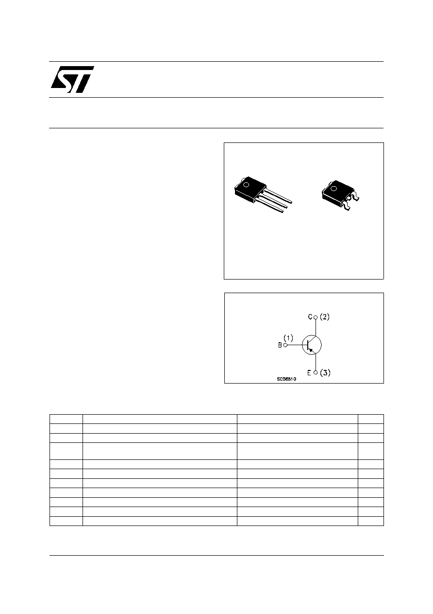
STD93003
HIGH VOLTAGE FAST-SWITCHING
PNP POWER TRANSISTOR
s
REVERSE PINS OUT Vs STANDARD IPAK
(TO-251) / DPAK (TO-252) PACKAGES
s
MEDIUM VOLTAGE CAPABILITY
s
LOW SPREAD OF DYNAMIC PARAMETERS
s
MINIMUM LOT-TO-LOT SPREAD FOR
RELIABLE OPERATION
s
VERY HIGH SWITCHING SPEED
s
SURFACE-MOUNTING DPAK (TO-252)
POWER PACKAGE IN TAPE & REEL (Suffix
"T4")
s
THROUGH-HOLE IPAK (TO-251) POWER
PACKAGE IN TUBE (Suffix "-1")
APPLICATIONS:
s
ELECTRONIC BALLASTS FOR
FLUORESCENT LIGHTING
DESCRIPTION
The device is manufactured using high voltage
Multi-Epitaxial Planar technology for high
switching speeds and medium voltage capability.
It uses a Cellular Emitter structure with planar
edge termination to enhance switching speeds
while maintaining the wide RBSOA.
The STD93003 is expressly designed for a new
solution to be used in compact fluorescent lamps,
where it is coupled with the STD83003, its
complementary NPN transistor.
Æ
INTERNAL SCHEMATIC DIAGRAM
October 2002
ABSOLUTE MAXIMUM RATINGS
Symbol
Parameter
Value
Unit
V
CES
Collector-Emitter Voltage (V
BE
= 0)
-500
V
V
CEO
Collector-Emitter Voltage (I
B
= 0)
-400
V
V
EBO
Emitter-Base Voltage
(I
C
= 0, I
B
= -0.75 A, t
p
< 10
µ
s, T
j
< 150
o
C)
V
(BR)EBO
V
I
C
Collector Current
-1.5
A
I
CM
Collector Peak Current (t
p
< 5 ms)
-3
A
I
B
Base Current
-0.75
A
I
BM
Base Peak Current (t
p
< 5 ms)
-1.5
A
P
tot
Total Dissipation at T
c
= 25
o
C
20
W
T
stg
Storage Temperature
-65 to 150
o
C
T
j
Max. Operating Junction Temperature
150
o
C
3
2
1
IPAK
TO-251
(Suffix "-1")
1
3
DPAK
TO-252
(Suffix "T4")
1/8
THERMAL DATA
R
thj-case
R
thj-amb
Thermal Resistance Junction-case Max
Thermal Resistance Junction-ambient Max
6.25
100
o
C/W
o
C/W
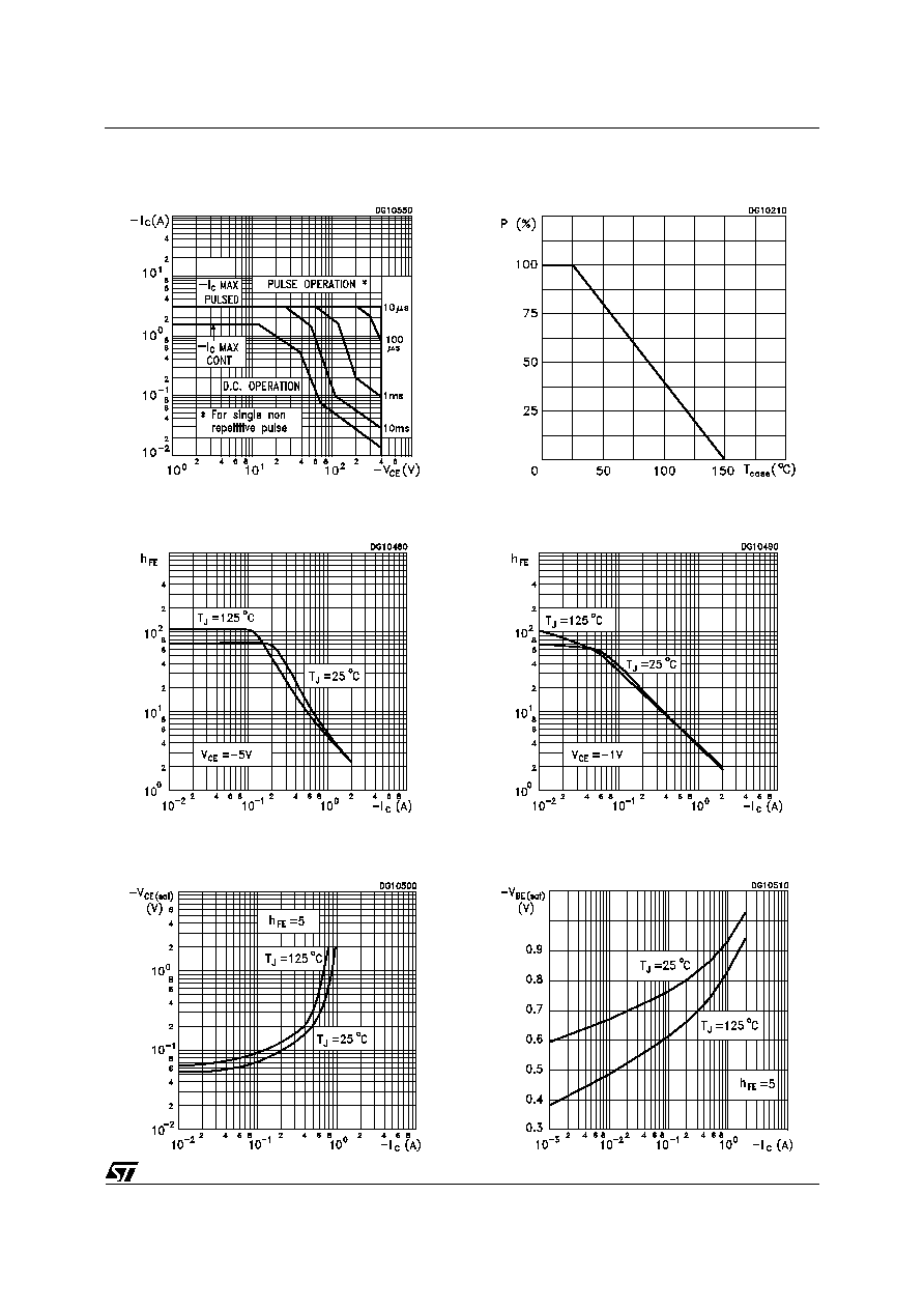
ELECTRICAL CHARACTERISTICS (T
case
= 25
o
C unless otherwise specified)
Symbol
Parameter
Test Conditions
Min.
Typ.
Max.
Unit
I
CES
Collector Cut-off
Current (V
BE
= 0)
V
CE
= -500V
V
CE
= -500V T
j
= 125
o
C
-1
-5
mA
mA
V
(BR)EBO
Emitter Base
Breakdown Voltage
(I
C
= 0)
I
E
= -10 mA
-5
-10
V
V
CEO(sus)
Collector-Emitter
Sustaining Voltage
(I
B
= 0)
I
C
= -10 mA
L = 25 mH
-400
V
V
CE(sat)
Collector-Emitter
Saturation Voltage
I
C
= -0.5 A I
B
= -0.1 A
I
C
= -0.35 A I
B
= -50 mA
-0.5
-0.5
V
V
V
BE(sat)
Base-Emitter
Saturation Voltage
I
C
= -0.5 A I
B
= -0.1 A
-1
V
h
FE
DC Current Gain
I
C
= -10 mA V
CE
= -5 V
I
C
= -0.35 A V
CE
= -5 V
I
C
= -1 A V
CE
= -5 V
10
16
4
25
32
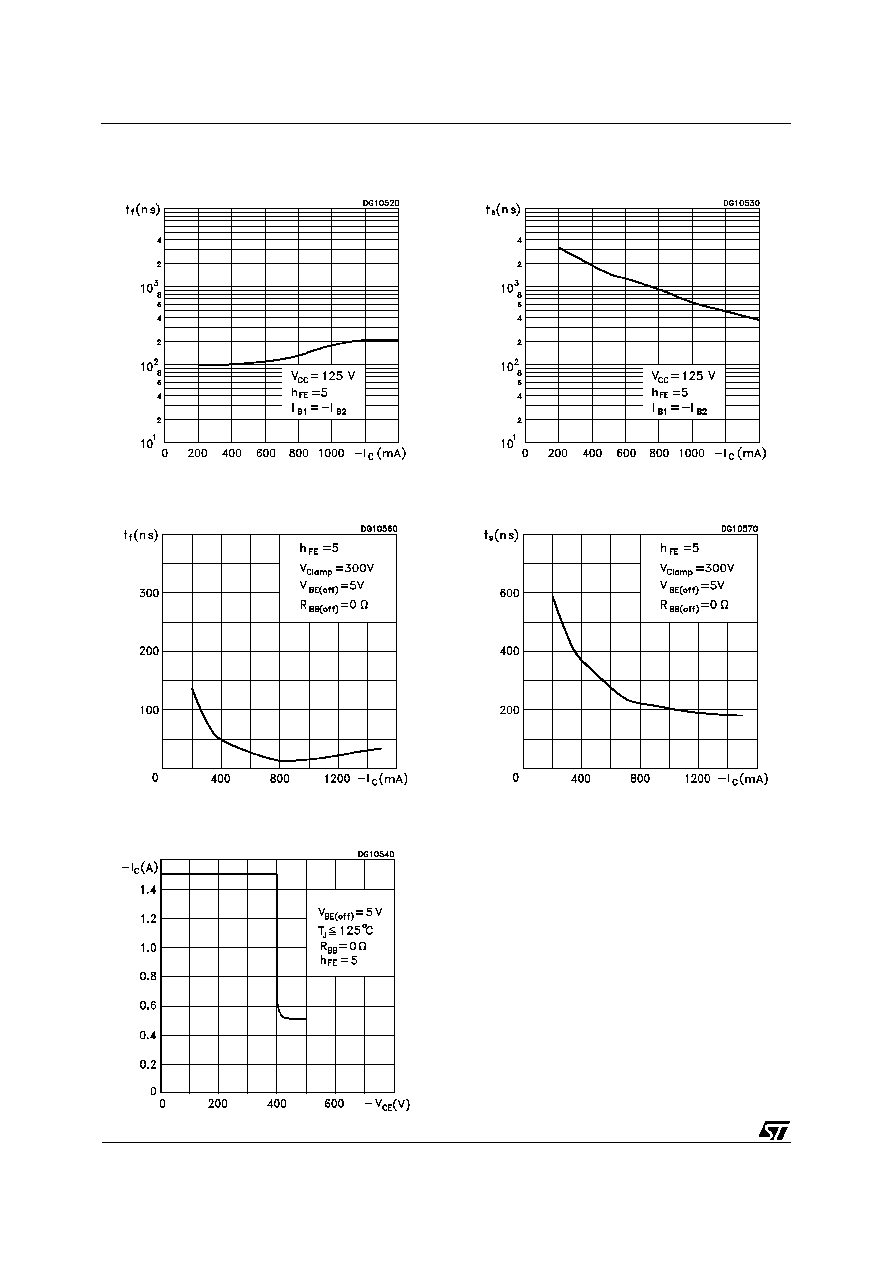
t
r
t
s
t
f
RESISTIVE LOAD
Rise Time
Storage Time
Fall Time
I
C
= -0.35 A V
CC
= 125 V
I
B1
= -70 mA I
B2
= 70 mA
T
p
25
µ
s (see Figure 2)
1.5
90
2.2
0.1
2.9
ns
µ
s
µ
s
t
s
t
f
INDUCTIVE LOAD
Storage Time
Fall Time
I
C
= -0.5 A I
B1
= -0.1 A
V
BE(o ff)
= 5 V L = 10 mH
V
clamp
= 300 V (see Figure 1)
400
40
ns
ns
E
sb
Avalanche Energy
L = 4 mH C = 1.8 nF
I
BR
2.5 A 25
o
C < T
C
< 125
o
C
12
mJ
Pulsed: Pulse duration = 300
µ
s, duty cycle = 1.5 %.
STD93003
2/8

Figure 1: Inductive Load Switching Test Circuit.
Figure 2: Resistive Load Switching Test Circuit.
1) Fast electronic switch
2) Non-inductive Resistor
3) Fast recovery rectifier
1) Fast electronic switch
2) Non-inductive Resistor
STD93003
5/8