STDID5B
N - CHANNEL 55V - 0.1
- 12A TO-252
STripFET
TM
POWER MOSFET
PRELIMINARY DATA
s
TYPICAL R
DS(on)
= 0.1
s
APPLICATION ORIENTED
CHARACTERIZATION
s
ADD SUFFIX "T4" FOR ORDERING IN TAPE
& REEL
DESCRIPTION
This Power MOSFET is the latest development of
STMicroelectronics unique "Single Feature
Size
TM
" strip-based process. The resulting transi-
stor shows extremely high packing density for low
on-resistance, rugged avalanche characteristics
and less critical alignment steps therefore a re-
markable manufacturing reproducibility.
APPLICATIONS
s
DC MOTOR CONTROL
s
DC-DC & DC-AC CONVERTERS
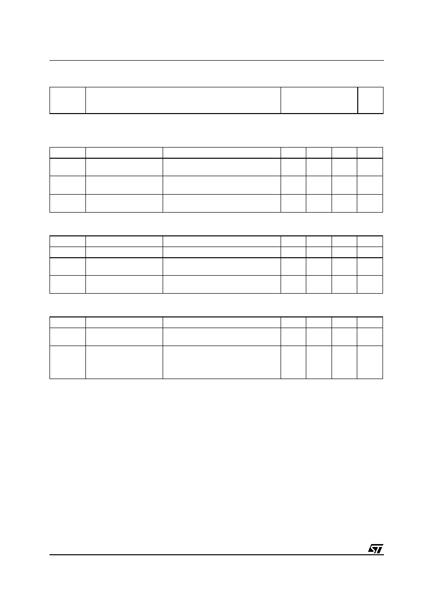
�
INTERNAL SCHEMATIC DIAGRAM
May 2000
ABSOLUTE MAXIMUM RATINGS
Symbol
Parameter
Value
Unit
V
DS
Drain-source Voltage (V
GS
= 0)
55
V
V
DGR
Drain- gate Voltage (R
GS
= 20 k
)
55
V
V
GS
Gate-source Voltage
�
20
V
I
D
(
*
)
Drain Current (continuous) at T
c
= 25
o
C
12
A
I
D
Drain Current (continuous) at T
c
= 100
o
C
8
A
I
DM
(
�
)
Drain Current (pulsed)
48
A
P
tot
Total Dissipation at T
c
= 25
o
C
35
W
Derating Factor
0.23
W/
o
C
E
AS
(1)
Single Pulse Avalanche Energy
25
mJ
T
st g
Storage Temperature
-65 to 175
o
C
T
j
Max. Operating Junction Temperature
175
o
C
(
�
) Pulse width limited by safe operating area
(
1
)
starting T
j
= 25
o
C, I
D
=12A , V
DD
= 30V New R
DS(on)
spec. starting from July '98
TYPE
V
DSS
R
DS(on)
I
D
STDID5B
55 V
< 0.12
12 A
1
3
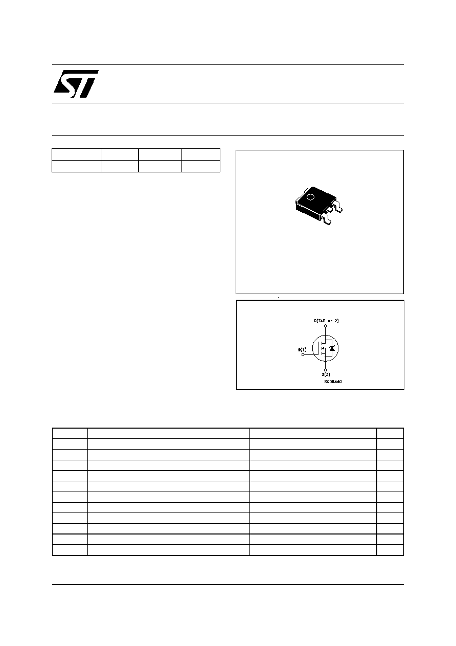
DPAK
TO-252
(Suffix "T4")
1/6
THERMAL DATA
R
thj-case
R
thj-amb
T
l
Thermal Resistance Junction-case Max
Thermal Resistance Junction-ambient Max
Maximum Lead Temperature For Soldering Purpose
4.3
100
275
o
C/W
o
C/W
o
C
ELECTRICAL CHARACTERISTICS (T
case
= 25
o
C unless otherwise specified)
OFF
Symbol
Parameter
Test Conditions
Min.
Typ.
Max.
Unit
V
(BR)DSS
Drain-source
Breakdown Voltage
I
D
= 250
�
A V
GS
= 0
55
V
I
DSS
Zero Gate Voltage
Drain Current (V
GS
= 0)
V
DS
= Max Rating
V
DS
= Max Rating T
c
= 125
o
C
1
10
�
A
�
A
I
GSS
Gate-body Leakage
Current (V
DS
= 0)
V
GS
=
�
20 V
�
100
nA
ON (
)
Symbol
Parameter
Test Conditions
Min.
Typ.
Max.
Unit
V
GS(th)
Gate Threshold Voltage V
DS
= V
GS
I
D
= 250
�
A
2
3
4
V
R
DS(on)
Static Drain-source On
Resistance
V
GS
= 10 V I
D
= 9.6 A
0.1
0.12
I
D(o n)
On State Drain Current
V
DS
> I
D(o n)
x R
DS(on )max
V
GS
= 10 V
12
A
DYNAMIC
Symbol
Parameter
Test Conditions
Min.
Typ.
Max.
Unit
g
fs
(
)
Forward
Transconductance
V
DS
> I
D(o n)
x R
DS(on )max
I
D
= 10 A
4
S
C
iss
C
oss
C
rss
Input Capacitance
Output Capacitance
Reverse Transfer
Capacitance
V
DS
= 25 V f = 1 MHz V
GS
= 0 V
360
55
25
pF
pF
pF
STDID5B
2/6
ELECTRICAL CHARACTERISTICS (continued)
SWITCHING ON
Symbol
Parameter
Test Conditions
Min.
Typ.
Max.
Unit
t
d(on )
t
r
Turn-on Delay Time
Rise Time
V
DD
= 30 V I
D
= 6 A
R
G
= 4.7
V
GS
= 10 V
(Resistive Load, see fig. 3)
10
25
ns
ns
Q
g
Q
gs
Q
gd
Total Gate Charge
Gate-Source Charge
Gate-Drain Charge
V
DD
= 48 V I
D
= 12 A V
GS
= 10 V
10
3.5
3.2
13.5
nC
nC
nC
SWITCHING OFF
Symbol
Parameter
Test Conditions
Min.
Typ.
Max.
Unit
t
d(of f)
t
f
Turn-off Delay Time
Fall Time
V
DD
= 30 V I
D
= 6 A
R
G
= 4.7
V
GS
= 10 V
(Resistive Load, see fig. 3)
31
8
ns
ns
SOURCE DRAIN DIODE
Symbol
Parameter
Test Conditions
Min.
Typ.
Max.
Unit
I
SD
I
SDM
(
�
)
Source-drain Current
Source-drain Current
(pulsed)
12
48
A
A
V
SD
(
)
Forward On Voltage
I
SD
= 12 A V
GS
= 0
1.3
V
t
rr
Q
rr
I
RRM
Reverse Recovery
Time
Reverse Recovery
Charge
Reverse Recovery
Current
I
SD
= 12 A di/dt = 100 A/
�
s
V
DD
= 30 V T
j
= 150
o
C
(see test circuit, fig. 5)
38
61
3.2
ns
nC
A
(
) Pulsed: Pulse duration = 300
�
s, duty cycle 1.5 %
(
�
) Pulse width limited by safe operating area
STDID5B
3/6
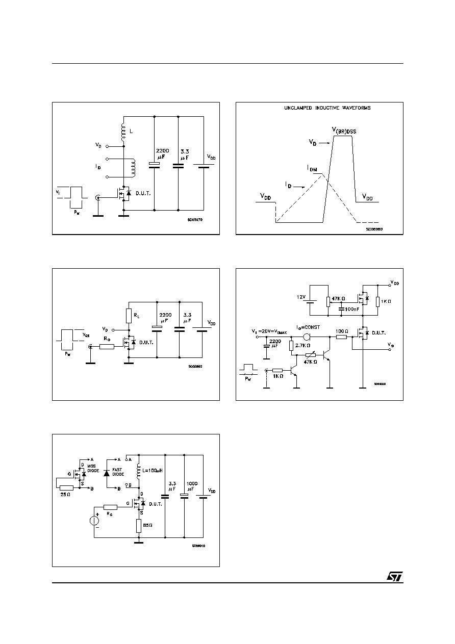
Fig. 1: Unclamped Inductive Load Test Circuit
Fig. 3: Switching Times Test Circuits For
Resistive Load
Fig. 2: Unclamped Inductive Waveform
Fig. 4: Gate Charge test Circuit
Fig. 5: Test Circuit For Inductive Load Switching
And Diode Recovery Times
STDID5B
4/6
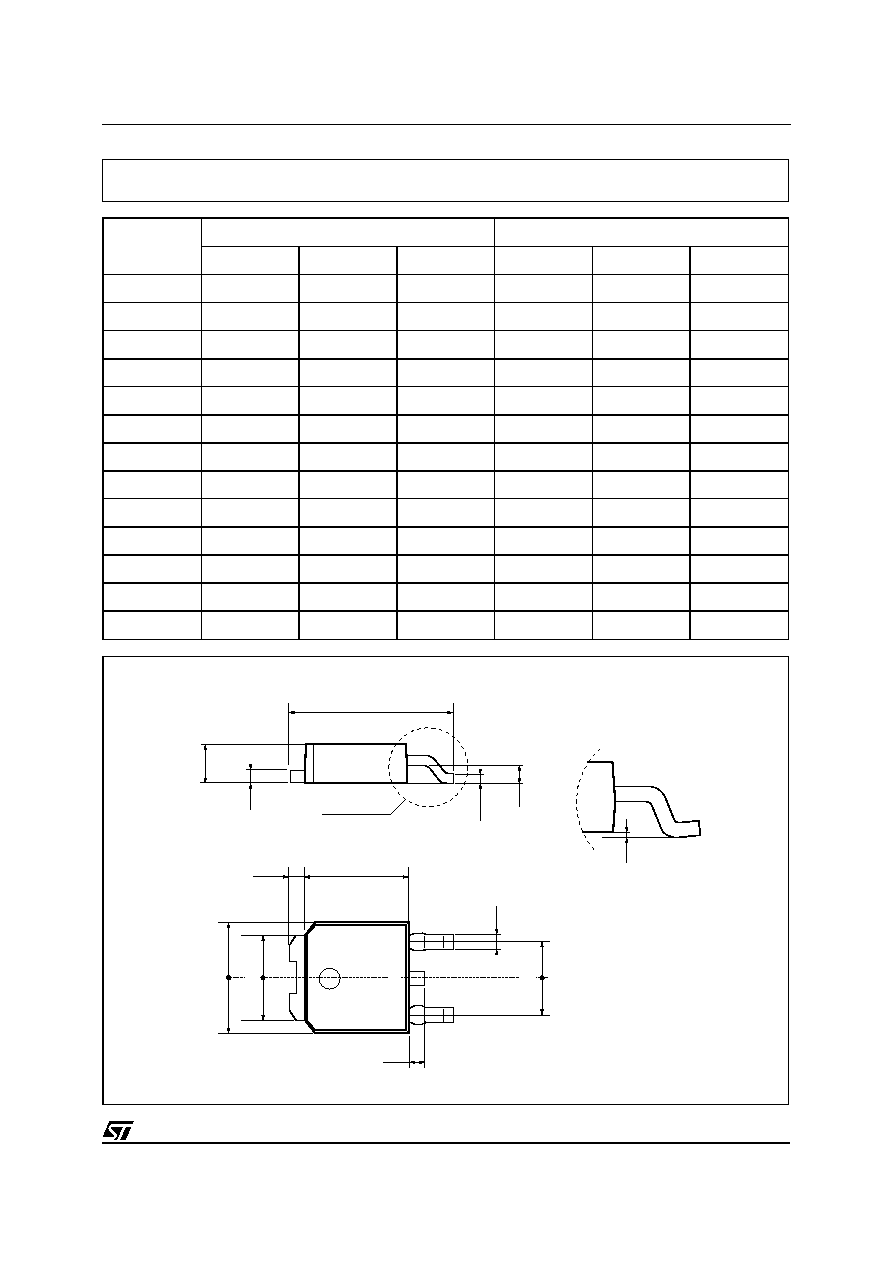
DIM.
mm
inch
MIN.
TYP.
MAX.
MIN.
TYP.
MAX.
A
2.2
2.4
0.086
0.094
A1
0.9
1.1
0.035
0.043
A2
0.03
0.23 0.001
0.009
B
0.64
0.9
0.025
0.035
B2
5.2
5.4
0.204
0.212
C
0.45
0.6
0.017
0.023
C2
0.48
0.6
0.019
0.023
D
6
6.2
0.236
0.244
E
6.4
6.6
0.252
0.260
G
4.4
4.6
0.173
0.181
H
9.35
10.1
0.368
0.397
L2
0.8
0.031
L4
0.6
1
0.023
0.039
==
D
L2
L4
1 3
==
B
E
==
B2
G
2
A
C2
C
H
A1
DETAIL "A"
A2
DETAIL "A"
TO-252 (DPAK) MECHANICAL DATA
0068772-B
STDID5B
5/6