STE15NA100
N - CHANNEL ENHANCEMENT MODE
FAST POWER MOS TRANSISTOR
PRELIMINARY DATA
s
TYPICAL R
DS(on)
= 0.65
s
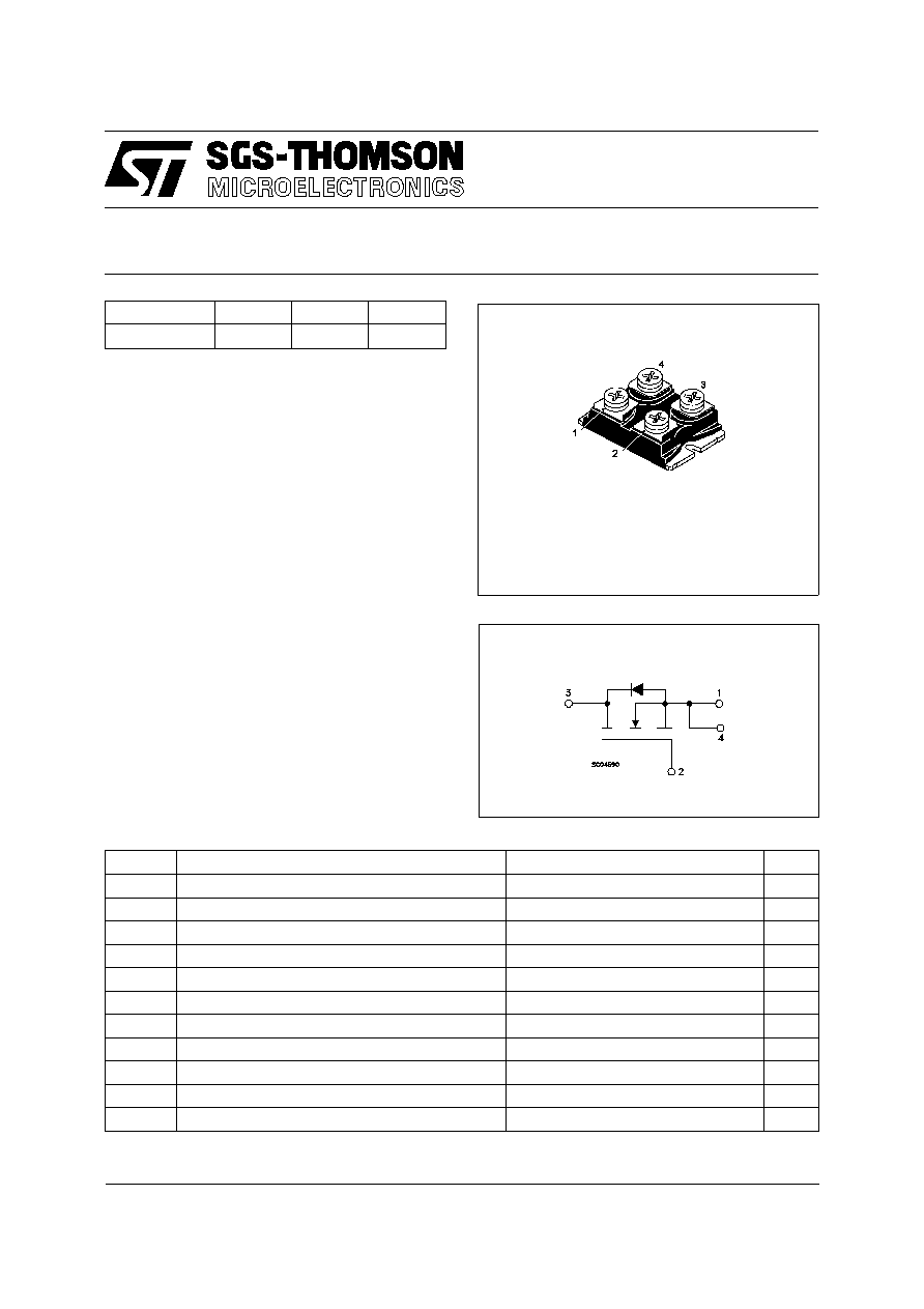
HIGH CURRENT POWER MODULE
s
AVALANCHE RUGGED TECHNOLOGY
s
VERY LARGE SOA - LARGE PEAK POWER
CAPABILITY
s
EASY TO MOUNT
s
SAME CURRENT CAPABILITY FOR THE
TWO SOURCE TERMINALS
s
EXTREMELY LOW Rth (Junction to case)
s
VERY LOW INTERNAL PARASITIC
INDUCTANCE
s
ISOLATED PACKAGE UL RECOGNIZED
APPLICATIONS
s
SMPS & UPS
s
MOTOR CONTROL
s
WELDING EQUIPMENT
s
OUTPUT STAGE FOR PWM, ULTRASONIC
CIRCUITS
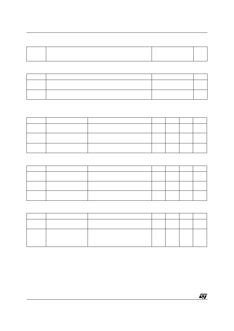
INTERNAL SCHEMATIC DIAGRAM
ABSOLUTE MAXIMUM RATINGS
Symbol
Parameter
Value
Unit
V
DS
Drain-source Voltage (V
GS
= 0)
1000
V
V
DGR
Drain- gate Voltage (R
GS
= 20 k
)
1000
V
V
GS
Gate-source Voltage
±
30
V
I
D
Drain Current (continuous) at T
c
= 25
o
C
15
A
I
D
Drain Current (continuous) at T
c
= 100
o
C
9.5
A
I
DM
(
∑
)
Drain Current (pulsed)
60
A
P
to t
Total Dissipation at T
c
= 25
o
C
300
W
Derating Factor
2.4
W/
o
C
T
stg
Storage Temperature
-55 to 150
o
C
T
j
Max. Operating Junction Temperature
150
o
C
V
ISO
Insulation Withhstand Voltage (AC-RMS)
2500
V
(
∑
) Pulse width limited by safe operating area
TYPE
V
DSS
R
DS(on)
I
D
STE15NA100
1000 V
< 0.77
15 A
February 1998
ISOTOP
1/5
THERMAL DATA
R
thj-case
R
thc-h
Thermal Resistance Junction-case Max
Thermal Resistance Case-heatsink With Conductive
Grease Applied Max
0.27
0.05
o
C/W
o
C/W
AVALANCHE CHARACTERISTICS
Symbol
Parameter
Max Value
Unit
I
AR
Avalanche Current, Repetitive or Not-Repetitive
(pulse width limited by T
j
max,
< 1%)
TBD
A
E
AS
Single Pulse Avalanche Energy
(starting T
j
= 25
o
C, I
D
= I
AR
, V
DD
= 50 V)
TBD
mJ
ELECTRICAL CHARACTERISTICS (T
case
= 25
o
C unless otherwise specified)
OFF
Symbol
Parameter
Test Conditions
Min.
Typ.
Max.
Unit
V
(BR)DSS
Drain-source
Breakdown Voltage
I
D
= 500
µ
A V
GS
= 0
1000
V
I
DSS
Zero Gate Voltage
Drain Current (V
GS
= 0)
V
DS
= Max Rating
V
DS
=0.8x Max Rating T
c
= 125
o
C
250
1000
µ
A
µ
A
I
GSS
Gate-body Leakage
Current (V
DS
= 0)
V
GS
=
±
30 V
±
200
nA
ON (
)
Symbol
Parameter
Test Conditions
Min.
Typ.
Max.
Unit
V
GS(th)
Gate Threshold
Voltage
V
DS
= V
GS
I
D
= 1mA
2.25
3
3.75
V
R
DS(on)
Static Drain-source On
Resistance
V
GS
= 10V I
D
= 7.5 A
0.65
0.77
I
D(on )
On State Drain Current V
DS
> I
D(on)
x R
DS(on)max
V
GS
= 10 V
15
A
DYNAMIC
Symbol
Parameter
Test Conditions
Min.
Typ.
Max.
Unit
g
fs
(
)
Forward
Transconductance
V
DS
> I
D(on)
x R
DS(on)max
I
D
= 7.5 A
12
S
C
iss
C
oss
C
rss
Input Capacitance
Output Capacitance
Reverse Transfer
Capacitance
V
DS
= 25 V f = 1.0 MHz V
GS
= 0
7
600
150
9.1
780
195
nF
pF
pF
STE15NA100
2/5
ELECTRICAL CHARACTERISTICS (continued)
SWITCHING ON
Symbol
Parameter
Test Conditions
Min.
Typ.
Max.
Unit
t
d(on)
t
r
Turn-on Time
Rise Time
V
DD
= 500 V I
D
= 7.5 A
R
G
= 4.7
V
GS
= 10 V
40
55
56
77
ns
ns
Q
g
Q
gs
Q
gd
Total Gate Charge
Gate-Source Charge
Gate-Drain Charge
V
DD
= 800 V I
D
= 15 A V
GS
= 10 V
470
43
226
660
nC
nC
nC
SWITCHING OFF
Symbol
Parameter
Test Conditions
Min.
Typ.
Max.
Unit
t
r(Voff)
t
f
t
c
Off-voltage Rise Time
Fall Time
Cross-over Time
V
DD
= 800 V I
D
= 15 A
R
G
= 4.7
V
GS
= 10 V
110
25
150
154
36
210
ns
ns
ns
SOURCE DRAIN DIODE
Symbol
Parameter
Test Conditions
Min.
Typ.
Max.
Unit
I
SD
I
SDM
(
∑
)
Source-drain Current
Source-drain Current
(pulsed)
15
60
A
A
V
SD
(
)
Forward On Voltage
I
SD
= 15 A V
GS
= 0
1.6
V
t
rr
Q
rr
I
RRM
Reverse Recovery
Time
Reverse Recovery
Charge
Reverse Recovery
Current
I
SD
= 15 A di/dt = 100 A/
µ
s
V
R
= 100 V T
j
= 150
o
C
1400
42
60
ns
µ
C
A
(
) Pulsed: Pulse duration = 300
µ
s, duty cycle 1.5 %
(
∑
) Pulse width limited by safe operating area
STE15NA100
3/5
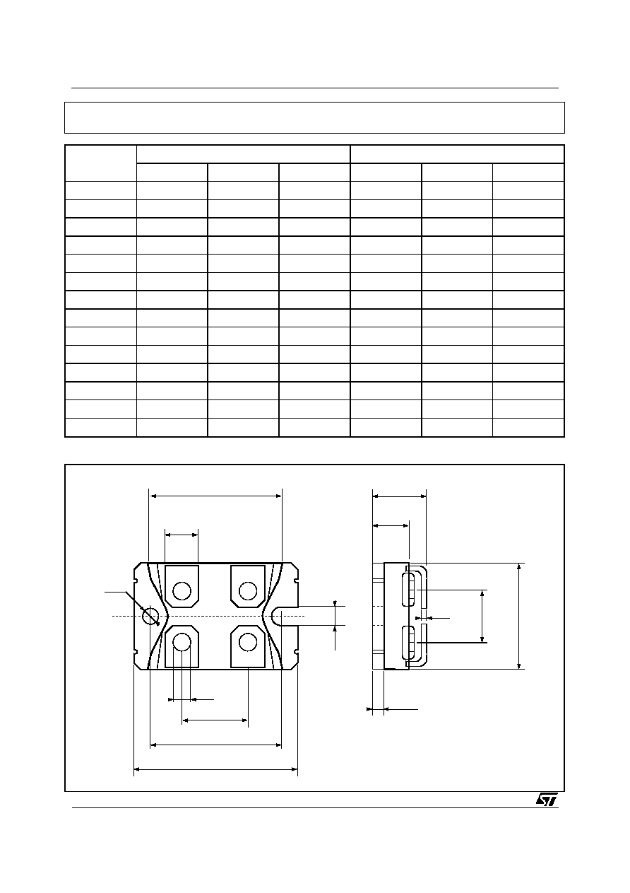
DIM.
mm
inch
MIN.
TYP.
MAX.
MIN.
TYP.
MAX.
A
11.8
12.2
0.466
0.480
B
8.9
9.1
0.350
0.358
C
1.95
2.05
0.076
0.080
D
0.75
0.85
0.029
0.033
E
12.6
12.8
0.496
0.503
F
25.15
25.5
0.990
1.003
G
31.5
31.7
1.240
1.248
H
4
0.157
J
4.1
4.3
0.161
0.169
K
14.9
15.1
0.586
0.594
L
30.1
30.3
1.185
1.193
M
37.8
38.2
1.488
1.503
N
4
0.157
O
7.8
8.2
0.307
0.322
B
E
H
O
N
J
K
L
M
F
A
C
G
D
ISOTOP MECHANICAL DATA
STE15NA100
4/5

Information furnished is believed to be accurate and reliable. However, SGS-THOMSON Microelectronics assumes no responsability for the
consequences of use of such information nor for any infringement of patents or other rights of third parties which may results from its use. No
license is granted by implication or otherwise under any patent or patent rights of SGS-THOMSON Microelectronics. Specifications mentioned
in this publication are subject to change without notice. This publication supersedes and replaces all information previously supplied.
SGS-THOMSON Microelectronics products are not authorized for use as critical components in life support devices or systems without express
written approval of SGS-THOMSON Microelectonics.
© 1998 SGS-THOMSON Microelectronics - Printed in Italy - All Rights Reserved
SGS-THOMSON Microelectronics GROUP OF COMPANIES
Australia - Brazil - Canada - China - France - Germany - Italy - Japan - Korea - Malaysia - Malta - Morocco - The Netherlands -
Singapore - Spain - Sweden - Switzerland - Taiwan - Thailand - United Kingdom - U.S.A
. . .
STE15NA100
5/5