 | –≠–ª–µ–∫—Ç—Ä–æ–Ω–Ω—ã–π –∫–æ–º–ø–æ–Ω–µ–Ω—Ç: STE2001 | –°–∫–∞—á–∞—Ç—å:  PDF PDF  ZIP ZIP |
1/36
STE2001
October 2001
This is preliminary information on a new product now in development. Details are subject to change without notice.
s
65 x 128 bits Display Data RAM
s
Configurable matrix: 65 x 128 or 33 x 128
s
Programmable (65/33) MUX rate
s
Row by Row Scrolling
s
Automatic data RAM Blanking procedure
s
Selectable Input Interface:
∑
I
2
C Bus Fast and Hs-mode (read and write)
∑
Parallel Interface (write only)
∑
Serial Interface (write only)
s
Fully Integrated Oscillator requires no external
components
s
Fully Integrated Configurable LCD bias voltages
generator with:
∑
Selectable (5X, 4X, 3X, 2X) multiplication factor
∑
Effective sensing for High Precision Output
∑
Four selectable temperature compensation
coefficients
s
Designed for chip-on-glass (COG) applications
s
Programmable bottom row pads mirroring and
top row pads mirroring for compatible with both
TCP and COG applications
s
Low Power Consumption, suitable for battery
operated systems
s
Logic Supply Voltage range from 1.9 to 5V
s
High Voltage Generator Supply Voltage range
from 2.4 to 4.5V
s
Display Supply Voltage range from 4.5 to 9V
DESCRIPTION
The STE2001 is a low power CMOS LCD controller
driver. Designed to drive a 65 rows by 128 columns
graphic display, provides all necessary functions in a
single chip, including on-chip LCD supply and bias
voltages generators, resulting in a minimum of exter-
nals components and in a very low power consump-
tion. The STE2001 features three standard interfaces
(Serial, parallel, I
2
C) for ease of interfacing with the
host
µ
controller.
Type
Ordering Number
Bumped Wafers
STE2001DIE1
Bumped Dice on Waffle Pack
STE2001DIE2
PRODUCT PREVIEW
65 X 128 SINGLE CHIP LCD CONTROLLER / DRIVER
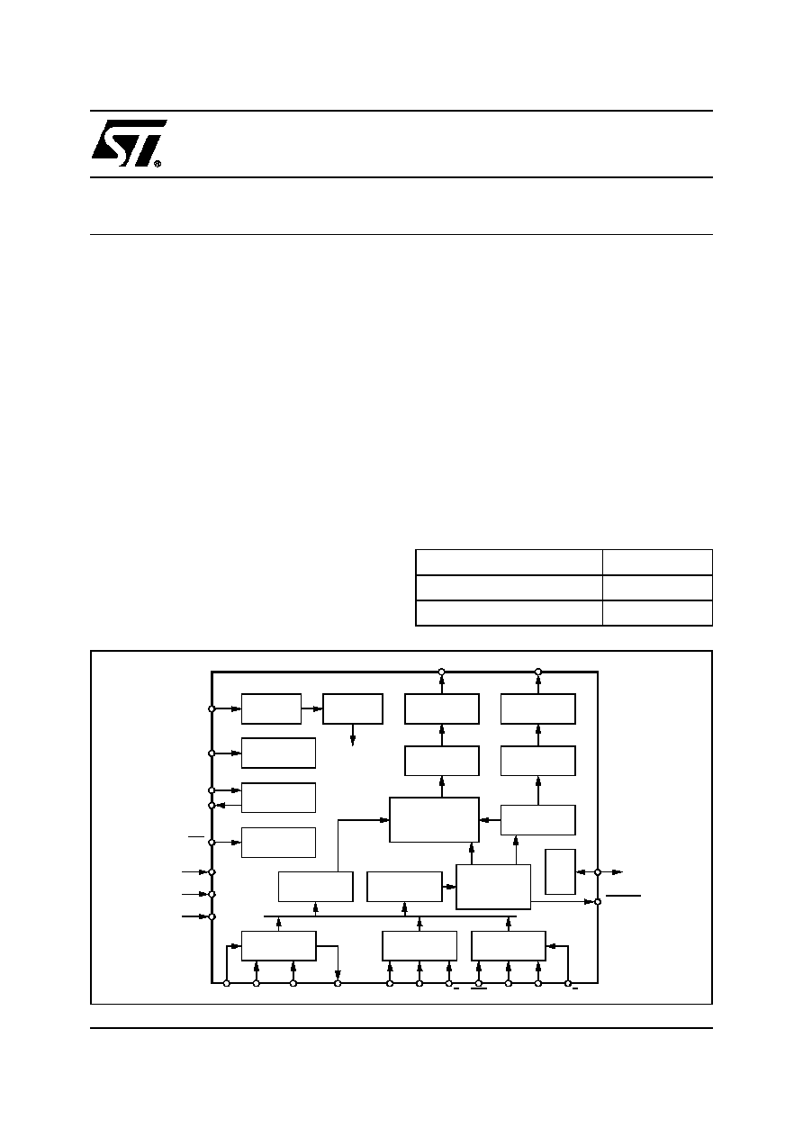
Figure 1. Block Diagram
COLUMN
DRIVERS
ROW
DRIVERS
DATA
LATCHES
65 x 128
RAM
DISPLAY
CONTROL
LOGIC
SCROLL
LOGIC
DATA
REGISTER
I2CBUS
INSTRUCTION
REGISTER
OSC
CO to C127
R0 to R64
OSC
VLCDIN
VLCDSENSE
RES
VDD1,2,3
CLOCK
TIMING
GENERATOR
BIAS VOLTAGE
GENERATOR
HIGH VOLTAGE
GENERATOR
RESET
TEST
SHIFT
REGISTER
VLCDOUT
V
SS
1,2
SEL1,2
SAO
TEST_0_13
SDA_IN
SDA_OUT
SCL
DB0 to DB7 E
PD/C
PARALLEL
SERIAL
D00IN1137
SCE
SDIN
SCLK
SD/C
BSY_FLG
STE2001
2/36
PIN DESCRIPTION
N
∞
Pad
Type
Function
R0 to R64
1 to 16
145 to 177
257 to 272
O
LCD Row Driver Output
C0 to C127
17 to 144
O
LCD Column Driver Output
V
SS1
,
2
227 to 238
GND
Ground pads. V
SS1
is GND for V
DD1
, V
SS2
for V
DD2
and V
DD3
V
DD1
186 to 191
Supply
IC Positive Power Supply
V
DD2
,
3
192 to 201
Supply
Internal Generator Supply Voltages.
V
LCDIN
246 to 251
Supply
LCD Supply Voltages for the Column and Row Output Drivers.
V
LCDOUT
239 to 244
Supply
Voltage Multiplier Ouput
V
LCDSENSE
245
Supply
Voltage Multiplier Regulation Input. V
LCDOUT
Sensing for Output Voltage Fine
Tuning
SEL1,2
183, 184
I
Interface Mode Selection
SDA_IN
223
I
I
2
C Bus Data In
SDA_OUT
222
O
I
2
C Bus Data Out
SCL
224
I
I
2
C bus Clock
SA0
225
I
I
2
C Slave Address LSB
OSC
185
I
External Oscillator Input
RES
221
I
Reset Input. Active Low.
DB0 to
DB7
211 to 218
I
Parallel Interface 8 Bit Data Bus
E
220
I
Parallel Interface Data Latch Signal. Data are Latched on the Falling EDGE.
PD/C
219
I
Parallel Interface Data/Command Selector
SDIN
207
I
Serial Interface Data Input
SCLK
210
I
Serial Interface Clock
SCE
209
I
Serial Interface ENABLE. When Low the Incoming Data are Clocked In.
SD/C
208
I
Serial Interface Data/Command selection
BSYFLG
206
O
Active Procedure Flag. Notice if There is an ongoing Internal Operation. Active
Low.
T1 to T13
178 to 181
202 to 205
226
252 to 256
I/O
Test Pads.
3/36
STE2001
ABSOLUTE MAXIMUM RATINGS
ELECTRICAL CHARACTERISTICS
DC OPERATION
(V
DD1
= 1.9 to V
DD2,3
+ 0.5V; V
DD2,3
= 2.4 to 4.5 V; V
ss1,2
= 0V; V
LCD
= 4.5 to 9V; T
amb
=-40 to 85
∞
C; unless otherwise
specified)
Symbol
Parameter
Value
Unit
V
DD1
Supply Voltage Range
- 0.5 to + 6.5
V
V
DD2,3
Supply Voltage Range
- 0.5 to + 5
V
V
LCD
LCD Supply Voltage Range
- 0.5 to + 10
V
I
SS
Supply Current
- 50 to +50
mA
V
i
Input Voltage (all input pads)
-0.5 to V
DD2,3
+ 0.5
V
I
in
DC Input Current
- 10 to + 10
mA
I
out
DC Output Current
- 10 to + 10
mA
P
tot
Total Power Dissipation (T
j
= 85
∞
C)
300
mW
P
o
Power Dissipation per Output
30
mW
T
j
Operating Junction Temperature
-40 to + 85
∞
C
T
stg
Storage Temperature
- 65 to 150
∞
C
Symbol
Parameter
Test Condition
Min.
Typ.
Max.
Unit
Supply Voltages
V
DD1
Supply Voltage
1.9
V
DD2,3
+ 0.5
V
T
amb
=-20 to 85
∞
C
1.8
V
DD2,3
+ 0.5
V
V
DD2,3
Supply Voltage
LCD Voltage Internally
generated
2.4
4.5
V
V
LCDIN
LCD Supply Voltage
LCD Voltage Supplied externally
4.5
9
V
V
LCDOUT
LCD Supply Voltage
Internally generated; note 1
4.5
9
V
I(V
DD1
)
Supply Current
V
DD
= 2.8V; V
LCD
= 7.6V; 4x
charge pump; f
sclk
= 0;
T
amb
= 25
∞
C; note 3.
8
15
µ
A
I(V
DD2,3
)
Voltage Generator Supply
Current
with VOP = 0 and PRS = 0
with external V
LCD
= 7.6V
10
15
µ
A
V
LCD
=7.6V; V
DD
=2.8V;
f
sclk
= 0; T
amb
= 25
∞
C; no display
load; 4x charge pump; note 3,6
F
osc
= 0
70
115
µ
A
STE2001
4/36
Notes: 1. The maximum possible V
LCD
voltage that can be generated is dependent on voltage, temperature and (display) load.
2. Internal clock
3. When f
sclk
= 0 there is no interface clock.
4. Power-down mode. During power-down all static currents are switched-off.
5. If external V
LCD
, the display load current is not transmitted to I
DD
6. Tolerance depends on the temperature; (typically zero at T
amb
= 27
∞
C), maximum tolerance values are measured at the temper-
ature range limit.
7. For TC0 to TC3
AC OPERATION
(V
DD1
= 1.9 to V
DD2,3
+ 0.5V; V
DD2,3
= 2.4 to 4.5 V; V
ss1,2
= 0V; V
LCD
= 4.5 to 9V; T
amb
=-40 to 85
∞
C; unless otherwise
specified)
I(V
DD1,2,3
)
Total Supply Current
V
LCD
= 7.6V; V
DD
=2.8V;
4x charge pump; f
sclk
= 0; T
amb
= 25
∞
C; no display load; note 3,6
F
osc
= 0
80
125
µ
A
I(V
LDCIN
)
External LCD Supply Voltage
Current
V
DD
=2.8V; V
LCD
=7.6V;no
display load; f
sclk
= 0;
T
amb
= 25
∞
C; note 3. F
osc
= 0
15
25
µ
A
Logic Inputs
V
IL
Logic LOW voltage level
V
IN
= V
ih
(t
p
< 10
µ
s)
V
SS
0.3
V
DD
V
V
IH
Logic HIGH Voltage Level
V
IN
= V
il
(t
p
< 10
µ
s)
0.7
V
DD
V
DD2,3
+ 0.5
V
I
in
Input Current
V
in
= V
SS1
or V
DD1
-1
1
µ
A
Column and Row Driver
R
row
ROW Output Resistance
12
20
kohm
R
col
Column Output resistance
12
20
kohm
V
col
Column Bias voltage accuracy
No load
-100
100
mV
V
row
Row Bias voltage accuracy
-100
100
mV
LCD Supply Voltage
V
LCD
LCD Supply Voltage accuracy;
Internally generated
V
DD
= 2.8V; V
LCD
= 7.6V;
fsclk=0; Tamb=25 C;
no display load; note 2, 3, 6 & 7
-300
300
mV
TC
Temperature coefficient
00
-550
PPM/
∞
C
01
-1350
PPM/
∞
C
10
-1650
PPM/
∞
C
11
-2650
PPM/
∞
C
Symbol
Parameter
Test Condition
Min.
Typ.
Max.
Unit
INTERNAL OSCILLATOR
F
OSC
Internal Oscillator frequency
V
DD
= 2.8V;
20
38
70
kHz
F
EXT
External Oscillator frequency
20
38
100
kHz
Symbol
Parameter
Test Condition
Min.
Typ.
Max.
Unit
ELECTRICAL CHARACTERISTICS (continued)
5/36
STE2001
F
FRAME
Frame frequency
fosc or fext = 38 kHz; note 1
73
Hz
T
VHRL
Vdd1 to RES Low
note 2 and 10; C
VLCD
= 1
µ
F
0
5
ms
T
w(RES)
RES LOW pulse width
note 3
600
ns
Reset Pulse Rejection
T
amb
= 25
∞
C; note 11
370
µ
s
Reset Pulse Rejection
note 11
200
µ
s
T
START
Reset Pulse vs. Device Ready
1
ms
T
VDD
0
I
2
C BUS INTERFACE (See note 4)
F
SCL
SCL Clock Frequency
Fast Mode ; V
DD1
=4.5V
DC
400
kHz
V
DD1
=18V; T
amb
= -20 to 70
∞
C
400
kHz
High Speed Mode; Cb=100pF
(max); note 6; V
DD1
=4.5V
DC
3.4
MHz
High Speed Mode; Cb=400pF
(max); note 6 ; V
DD1
=4.5V
DC
1.7
MHz
T
SCLL
Cb=100pF
160
ns
T
SCLH
Cb=100pF
160
ns
T
SCLL
Cb=400pF
320
ns
T
SCLH
Cb=400pF
320
ns
T
SU;DAT
Cb=100pF
30
ns
T
HD;DAT
Cb=100pF
30
ns
T
SU;DAT
Cb=400pF
30
ns
T
HD;DAT
Cb=400pF
30
ns
T
SU;STA
Cb=100pF
Note 8
170
ns
T
SU;STA
Cb=400pF
Note 8
330
ns
T
HD;STA
Cb=100pF
Note 8
170
ns
T
HD;STA
Cb=400pF
Note 8
330
ns
T
SU;STO
Cb=100pF
Note 8
170
ns
T
SU;STO
Cb=400pF
Note 8
330
ns
T
rCL
Cb=100pF
Note 5, 8
25
ns
T
rCL
Cb=400pF
Note 5, 8
50
ns
T
rCL1
Cb=100pF
Note 5, 8
30
ns
T
rCL1
Cb=400pF
Note 5, 8
120
ns
T
rDA
Cb=100pF
Note 5, 8
30
ns
T
rDA
Cb=400pF
Note 5, 8
120
ns
T
fCL
Cb=100pF
Note 5, 8
25
ns
T
fCL
Cb=400pF
Note 5, 8
50
ns
Symbol
Parameter
Test Condition
Min.
Typ.
Max.
Unit
ELECTRICAL CHARACTERISTICS (continued)