STE24NA100
N - CHANNEL 1000V - 0.35
- 24A - ISOTOP
FAST POWER MOSFET
s
TYPICAL R
DS(on)
= 0.35
s
±
30V GATE TO SOURCE VOLTAGE RATING
s
100% AVALANCHE TESTED
s
LOW INTRINSIC CAPACITANCE
s
GATE CHARGE MINIMIZED
s
REDUCED VOLTAGE SPREAD
APPLICATIONS
s
HIGH CURRENT, HIGH SPEED SWITCHING
s
SWITCH MODE POWER SUPPLY (SMPS)
s
DC-AC CONVERTER FOR WELDING
EQUIPMENT AND UNINTERRUPTABLE
POWER SUPPLY AND MOTOR DRIVE
Æ
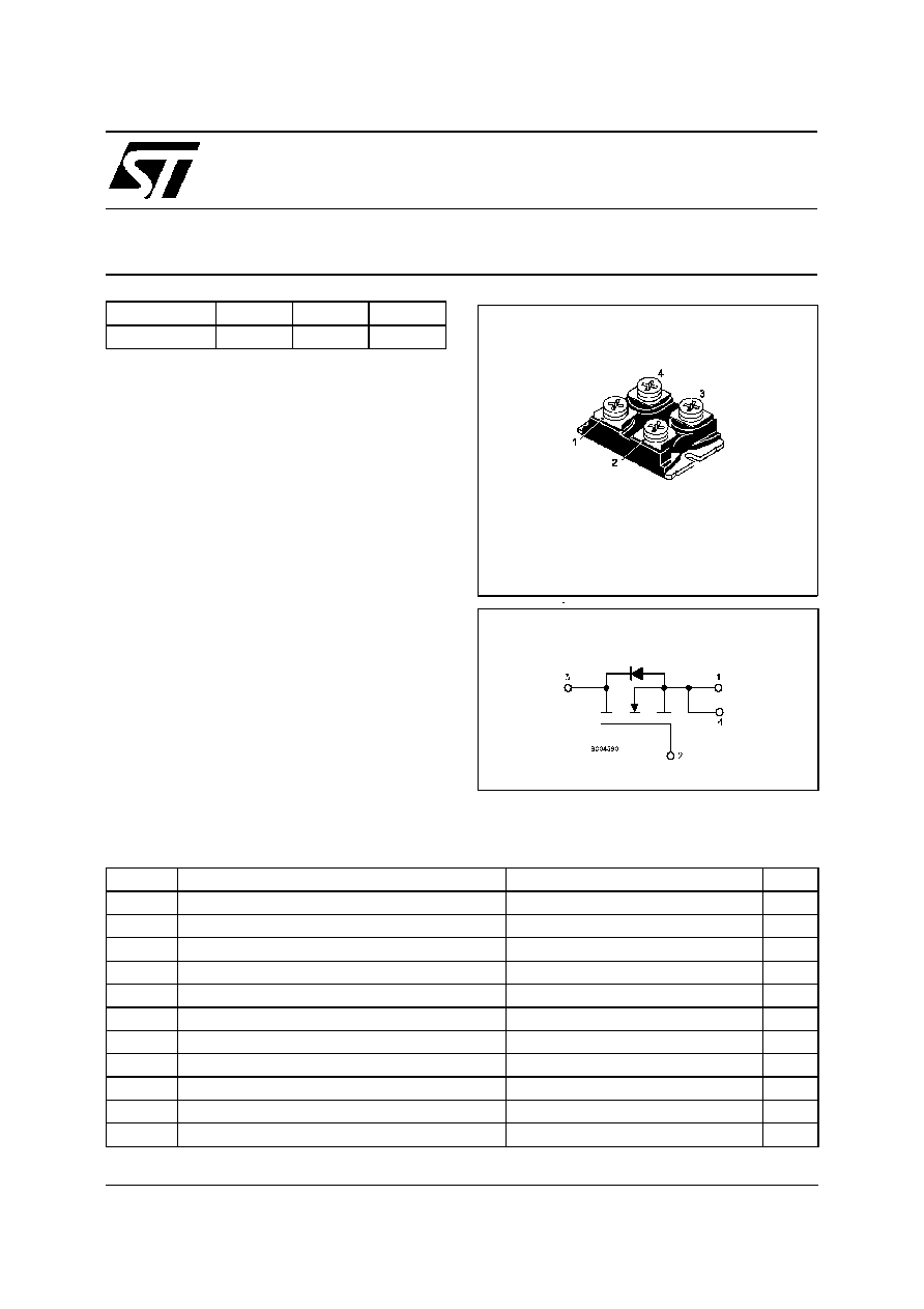
INTERNAL SCHEMATIC DIAGRAM
October 1998
ABSOLUTE MAXIMUM RATINGS
Symb ol
Parameter
Value
Un it
V
DS
Drain-source Volt age (V
GS
= 0)
1000
V
V
DGR
Drain- gate Voltage (R
GS
= 20 k
)
1000
V
V
GS
G ate-source Voltage
±
30
V
I
D
Drain Current (continuous) at T
c
= 25
o
C
24
A
I
D
Drain Current (continuous) at T
c
= 100
o
C
15
A
I
DM
(
∑
)
Drain Current (pulsed)
96
A
P
tot
T otal Dissipation at T
c
= 25
o
C
450
W
Derating Fact or
3.6
W /
o
C
T
s tg
Storage T emperature
-55 t o 150
o
C
T
j
Max. Operating Junction Temperat ure
150
o
C
V
ISO
I nsulation Withstand Voltage (AC-RMS)
2500
V
(
∑
) Pulse width limited by safe operating area
TYPE
V
DSS
R
DS(on)
I
D
STE24NA100
1000 V
< 0.385
24 A
ISOTOP
1/8
THERMAL DATA
R
thj -case
R
thc-h
Thermal Resistance Junction-case
Max
Thermal Resistance Case-heat sink With Conductive
Grease Applied
Max
0.27
0.05
o
C/W
o
C/W
AVALANCHE CHARACTERISTICS
Symbo l
Parameter
Max Value
Unit
I
AR
Avalanche Current, Repetitive or Not-Repetitive
(pulse width limited by T
j
max)
12
A
E
AS
Single Pulse Avalanche Energy
(starting T
j
= 25
o
C, I
D
= I
AR
, V
DD
= 50 V)
2000
mJ
ELECTRICAL CHARACTERISTICS (T
case
= 25
o
C unless otherwise specified)
OFF
Symbo l
Parameter
Test Con ditions
Min.
Typ.
Max.
Unit
V
(BR)DSS
Drain-source
Breakdown Voltage
I
D
= 500
µ
A
V
GS
= 0
1000
V
I
DSS
Zero Gat e Voltage
Drain Current (V
GS
= 0)
V
DS
= Max Rat ing
V
DS
= Max Rat ing
T
c
= 125
o
C
50
250
µ
A
µ
A
I
G SS
Gat e-body Leakage
Current (V
DS
= 0)
V
GS
=
±
30 V
±
400
nA
ON (
)
Symbo l
Parameter
Test Con ditions
Min.
Typ.
Max.
Unit
V
G S(th)
Gat e Threshold Voltage V
DS
= V
GS
I
D
= 1 mA
2.25
3
3.75
V
R
DS(on)
Static Drain-source On
Resistance
V
GS
= 10 V
I
D
= 12 A
0.35
0.385
I
D(o n)
On State Drain Current
V
DS
> I
D(o n)
x R
DS(on )ma x
V
GS
= 10 V
24
A
DYNAMIC
Symbo l
Parameter
Test Con ditions
Min.
Typ.
Max.
Unit
g
f s
(
)
Forward
Transconductance
V
DS
> I
D(o n)
x R
DS(on )ma x
I
D
= 12 A
15
S
C
iss
C
os s
C
rss
Input Capacitance
Out put Capacitance
Reverse Transfer
Capacitance
V
DS
= 25 V
f = 1 MHz
V
GS
= 0
14000
1200
300
19000
1600
390
pF
pF
pF
STE24NA100
2/8
ELECTRICAL CHARACTERISTICS (continued)
SWITCHING ON
Symbo l
Parameter
Test Con ditions
Min.
Typ.
Max.
Unit
t
d(on)
t
r
Turn-on Time
Rise Time
V
DD
= 500 V
I
D
= 12 A
R
G
= 4.7
V
G S
= 10 V
(see t est circuit, f igure 3)
40
55
56
77
ns
ns
Q
g
Q
gs
Q
gd
Tot al G ate Charge
Gat e-Source Charge
Gat e-Drain Charge
V
DD
= 800 V I
D
= 24 A V
GS
= 10 V
470
43
226
660
nC
nC
nC
SWITCHING OFF
Symbo l
Parameter
Test Con ditions
Min.
Typ.
Max.
Unit
t
r (Voff)
t
f
t
c
Off -volt age Rise T ime
Fall T ime
Cross-over Time
V
DD
= 800 V
I
D
= 24 A
R
G
= 4.7
V
G S
= 10 V
(see t est circuit, f igure 5)
110
25
150
154
35
210
ns
ns
ns
SOURCE DRAIN DIODE
Symbo l
Parameter
Test Con ditions
Min.
Typ.
Max.
Unit
I
SD
I
SDM
(
∑
)
Source-drain Current
Source-drain Current
(pulsed)
24
96
A
A
V
SD
(
)
Forward On Voltage
I
SD
= 24 A
V
GS
= 0
1. 6
V
t
rr
Q
rr
I
RRM
Reverse Recovery
Time
Reverse Recovery
Charge
Reverse Recovery
Current
I
SD
= 24 A
di/dt = 100 A/
µ
s
V
DD
= 100 V
T
j
= 150
o
C
(see t est circuit, f igure 5)
1.4
41
60
µ
s
µ
C
A
(
) Pulsed: Pulse duration = 300
µ
s, duty cycle 1.5 %
(
∑
) Pulse width limited by safe operating area
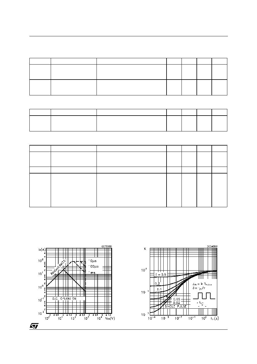
Safe Operating Area
Thermal Impedance
STE24NA100
3/8
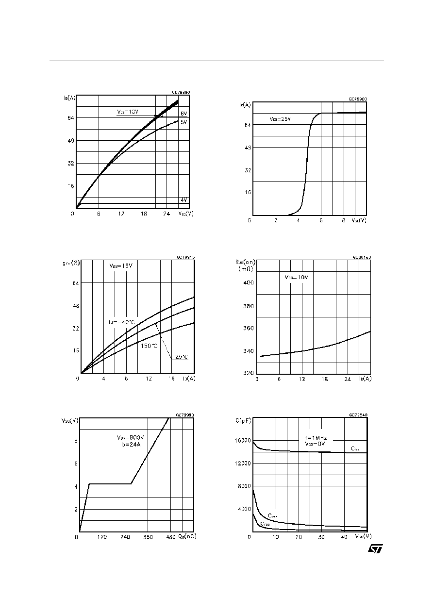
Output Characteristics
Transconductance
Gate Charge vs Gate-source Voltage
Transfer Characteristics
Static Drain-source On Resistance
Capacitance Variations
STE24NA100
4/8
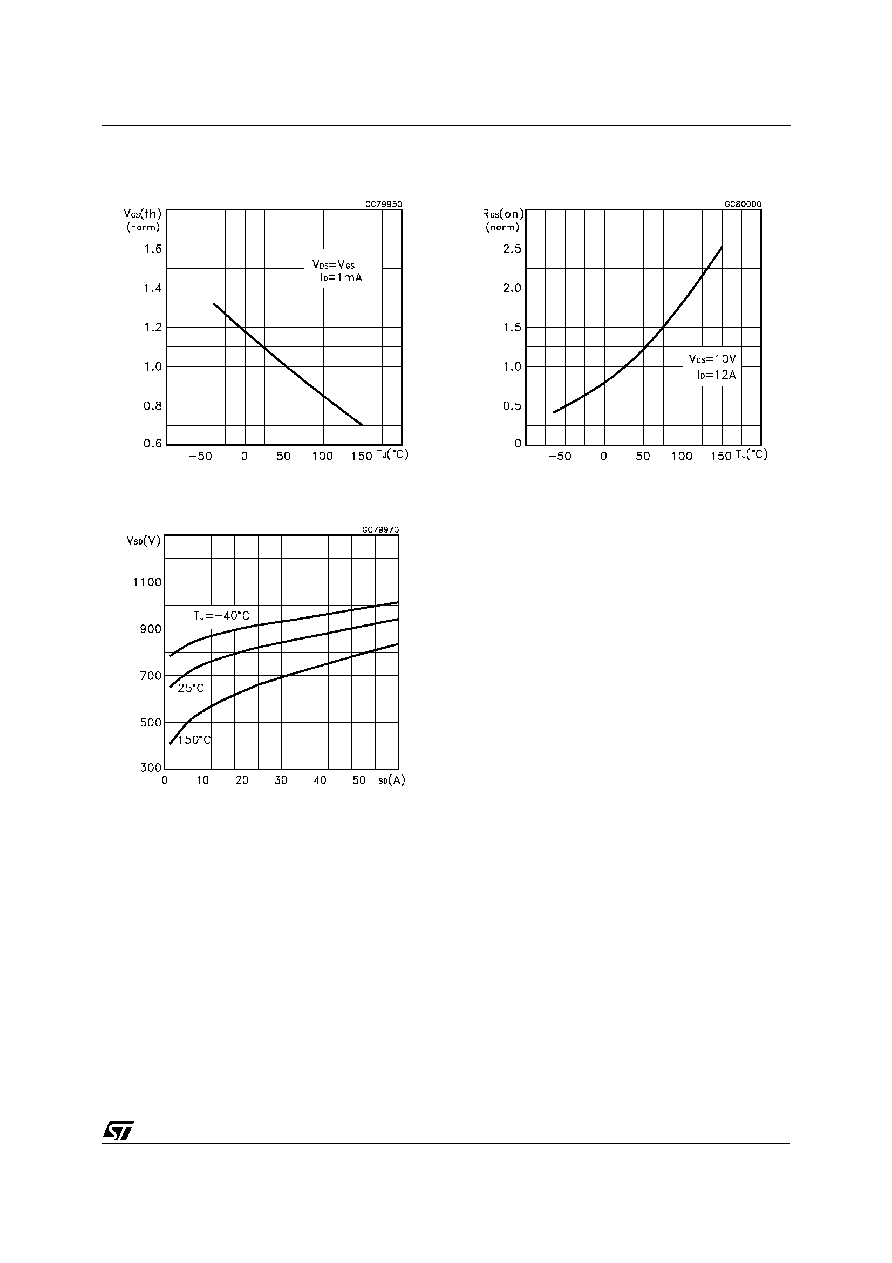
Normalized Gate Threshold Voltage vs
Temperature
Source-drain Diode Forward Characteristics
Normalized On Resistance vs Temperature
STE24NA100
5/8
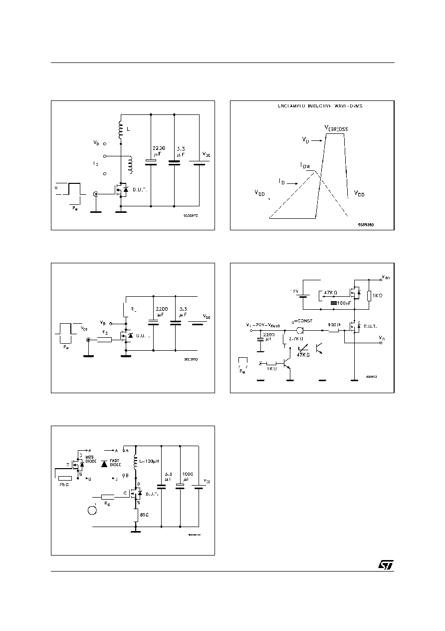
Fig. 1: Unclamped Inductive Load Test Circuit
Fig. 3: Switching Times Test Circuits For
Resistive Load
Fig. 2: Unclamped Inductive Waveform
Fig. 4: Gate Charge test Circuit
Fig. 5: Test Circuit For Inductive Load Switching
And Diode Recovery Times
STE24NA100
6/8
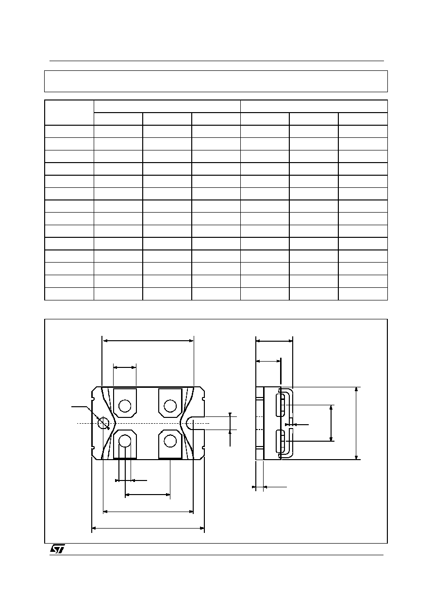
DIM.
mm
inch
MIN.
TYP.
MAX.
MIN.
TYP.
MAX.
A
11.8
12.2
0.466
0.480
B
8.9
9.1
0.350
0.358
C
1.95
2.05
0.076
0.080
D
0.75
0.85
0.029
0.033
E
12.6
12.8
0.496
0.503
F
25.15
25.5
0.990
1.003
G
31.5
31.7
1.240
1.248
H
4
0.157
J
4.1
4.3
0.161
0.169
K
14.9
15.1
0.586
0.594
L
30.1
30.3
1.185
1.193
M
37.8
38.2
1.488
1.503
N
4
0.157
O
7.8
8.2
0.307
0.322
B
E
H
O
N
J
K
L
M
F
A
C
G
D
ISOTOP MECHANICAL DATA
STE24NA100
7/8

Information furnished is believed to be accurate and reliable. However, STMicroelectronics assumes no responsibility for the consequences
of use of such information nor for any infringement of patents or other rights of third parties which may result from its use. No license is
granted by implication or otherwise under any patent or patent rights of STMicroelectronics. Specification mentioned in this publication are
subject to change without notice. This publication supersedes and replaces all information previously supplied. STMicroelectronics products
are not authorized for use as critical components in life support devices or systems without express written approval of STMicroelectronics.
The ST logo is a trademark of STMicroelectronics
©
1998 STMicroelectronics ≠ Printed in Italy ≠ All Rights Reserved
STMicroelectronics GROUP OF COMPANIES
Australia - Brazil - Canada - China - France - Germany - Italy - Japan - Korea - Malaysia - Malta - Mexico - Morocco - The Netherlands -
Singapore - Spain - Sweden - Switzerland - Taiwan - Thailand - United Kingdom - U.S.A.
http://www.st.com
.
STE24NA100
8/8