STE38NB50F
N - CHANNEL 500V - 0.11
- 38A - ISOTOP
PowerMESH
TM
MOSFET
s
TYPICAL R
DS(on)
= 0.11
s
EXTREMELY HIGH dv/dt CAPABILITY
s
±
30V GATE TO SOURCE VOLTAGE RATING
s
100% AVALANCHE TESTED
s
LOW INTRINSIC CAPACITANCE
s
GATE CHARGE MINIMIZED
s
REDUCED VOLTAGE SPREAD
DESCRIPTION
Using the latest high voltage MESH OVERLAY
TM
process, STMicroelectronics has designed an ad-
vanced family of power MOSFETs with outstand-
ing performances. The new patent pending strip
layout coupled with the Company's proprietary
edge termination structure, gives the lowest
RDS(on) per area, exceptional avalanche and
dv/dt capabilities and unrivalled gate charge and
switching characteristics.
APPLICATIONS
s
HIGH CURRENT, HIGH SPEED SWITCHING
s
SWITCH MODE POWER SUPPLY (SMPS)
s
DC-AC CONVERTER FOR WELDING
EQUIPMENT AND UNINTERRUPTABLE
POWER SUPPLY AND MOTOR DRIVE
Æ
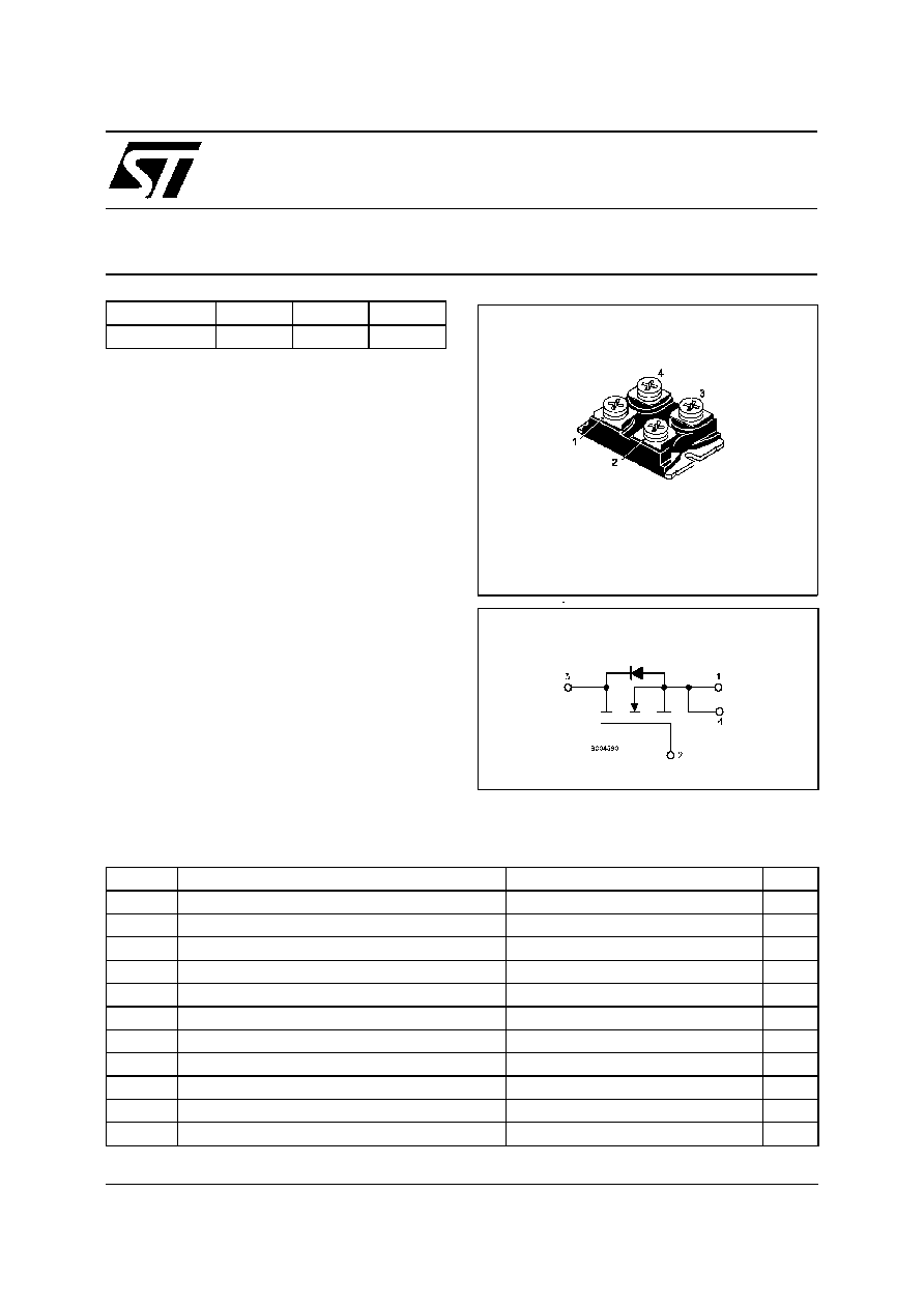
INTERNAL SCHEMATIC DIAGRAM
December 1999
ABSOLUTE MAXIMUM RATINGS
Symb ol
Parameter
Value
Un it
V
DS
Drain-source Volt age (V
GS
= 0)
500
V
V
DGR
Drain- gate Voltage (R
GS
= 20 k
)
500
V
V
GS
G ate-source Voltage
±
30
V
I
D
Drain Current (continuous) at T
c
= 25
o
C
38
A
I
D
Drain Current (continuous) at T
c
= 100
o
C
24
A
I
DM
(
∑
)
Drain Current (pulsed)
152
A
P
tot
T otal Dissipation at T
c
= 25
o
C
400
W
Derating Fact or
3.2
W /
o
C
dv/dt
(1)
Peak Diode Recovery voltage slope
4.5
V/ns
T
s tg
Storage T emperature
-65 t o 150
o
C
T
j
Max. Operating Junction Temperat ure
150
o
C
(
∑
) Pulse width limited by safe operating area
(
1
) I
SD
38 A, di/dt
200 A/
µ
s, V
DD
V
(BR)DSS
, T
j
T
JMAX
TYPE
V
DSS
R
DS(on)
I
D
STE38NB50F
500 V
< 0.14
38 A
ISOTOP
1/8
THERMAL DATA
R
thj -case
R
thj -amb
R
thc-sink
T
l
Thermal Resistance Junction-case
Max
Thermal Resistance Junction-ambient
Max
Thermal Resistance Case-sink
T yp
Maximum Lead Temperature F or Soldering Purpose
0.31
30
0.1
300
o
C/W
o
C/W
o
C/W
o
C
AVALANCHE CHARACTERISTICS
Symbo l
Parameter
Max Value
Unit
I
AR
Avalanche Current, Repetitive or Not-Repetitive
(pulse width limited by T
j
max)
38
A
E
AS
Single Pulse Avalanche Energy
(starting T
j
= 25
o
C, I
D
= I
AR
, V
DD
= 50 V)
1200
mJ
ELECTRICAL CHARACTERISTICS (T
case
= 25
o
C unless otherwise specified)
OFF
Symbo l
Parameter
Test Con ditions
Min.
Typ.
Max.
Unit
V
(BR)DSS
Drain-source
Breakdown Voltage
I
D
= 250
µ
A
V
GS
= 0
500
V
I
DSS
Zero Gat e Voltage
Drain Current (V
GS
= 0)
V
DS
= Max Rat ing
V
DS
= Max Rat ing
T
c
= 125
o
C
10
100
µ
A
µ
A
I
G SS
Gat e-body Leakage
Current (V
DS
= 0)
V
GS
=
±
30 V
±
100
nA
ON (
)
Symbo l
Parameter
Test Con ditions
Min.
Typ.
Max.
Unit
V
G S(th)
Gat e Threshold Voltage V
DS
= V
GS
I
D
= 250
µ
A
3
4
5
V
R
DS(on)
Static Drain-source On
Resistance
V
GS
= 10 V
I
D
= 19 A
0.11
0.14
I
D(o n)
On State Drain Current
V
DS
> I
D(o n)
x R
DS(on )ma x
V
GS
= 10 V
38
A
DYNAMIC
Symbo l
Parameter
Test Con ditions
Min.
Typ.
Max.
Unit
g
f s
(
)
Forward
Transconductance
V
DS
> I
D(o n)
x R
DS(on )ma x
I
D
= 19 A
27
S
C
iss
C
os s
C
rss
Input Capacitance
Out put Capacitance
Reverse Transfer
Capacitance
V
DS
= 25 V
f = 1 MHz
V
GS
= 0
5900
880
80
pF
pF
pF
STE38NB50F
2/8
ELECTRICAL CHARACTERISTICS (continued)
SWITCHING ON
Symbo l
Parameter
Test Con ditions
Min.
Typ.
Max.
Unit
t
d(on)
t
r
Turn-on Time
Rise Time
V
DD
= 250 V
I
D
= 19 A
R
G
= 4.7
V
G S
= 10 V
(see t est circuit, f igure 3)
45
35
ns
ns
Q
g
Q
gs
Q
gd
Tot al G ate Charge
Gat e-Source Charge
Gat e-Drain Charge
V
DD
= 400 V I
D
= 38 A V
GS
= 10 V
140
38
61
196
nC
nC
nC
SWITCHING OFF
Symbo l
Parameter
Test Con ditions
Min.
Typ.
Max.
Unit
t
r (Voff)
t
f
t
c
Off -volt age Rise T ime
Fall T ime
Cross-over Time
V
DD
= 400 V
I
D
= 38 A
R
G
= 4.7
V
G S
= 10 V
(see t est circuit, f igure 5)
28
30
60
ns
ns
ns
SOURCE DRAIN DIODE
Symbo l
Parameter
Test Con ditions
Min.
Typ.
Max.
Unit
I
SD
I
SDM
(
∑
)
Source-drain Current
Source-drain Current
(pulsed)
38
152
A
A
V
SD
(
)
Forward On Voltage
I
SD
= 38 A
V
GS
= 0
1. 6
V
t
rr
Q
rr
I
RRM
Reverse Recovery
Time
Reverse Recovery
Charge
Reverse Recovery
Current
I
SD
= 38 A
di/dt = 100 A/
µ
s
V
DD
= 100 V
T
j
= 150
o
C
(see t est circuit, f igure 5)
715
11.8
33
ns
µ
C
A
(
) Pulsed: Pulse duration = 300
µ
s, duty cycle 1.5 %
(
∑
) Pulse width limited by safe operating area
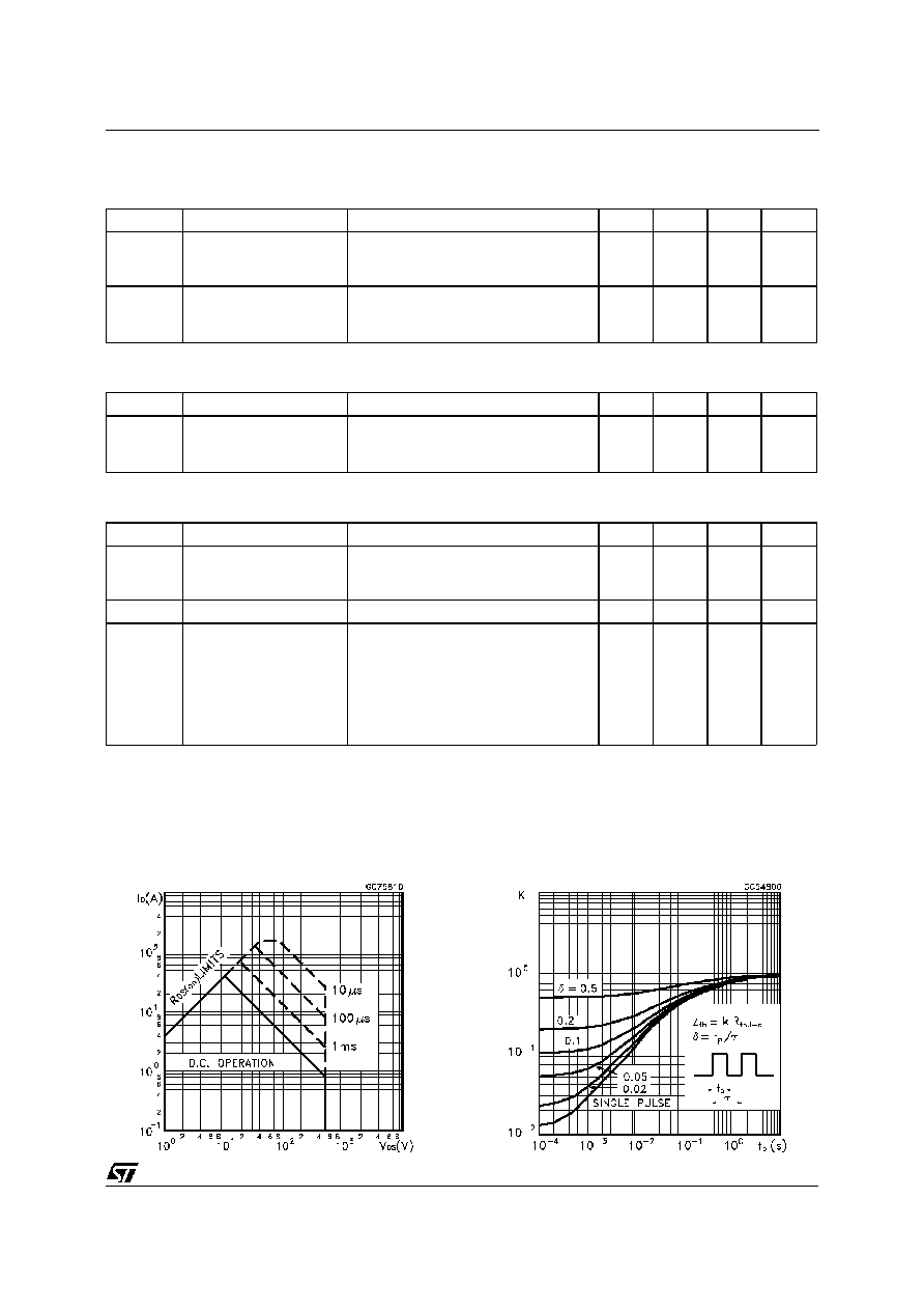
Safe Operating Area
Thermal Impedance
STE38NB50F
3/8
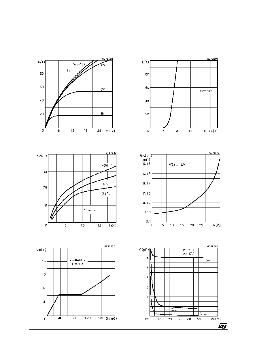
Output Characteristics
Transconductance
Gate Charge vs Gate-source Voltage
Transfer Characteristics
Static Drain-source On Resistance
Capacitance Variations
STE38NB50F
4/8
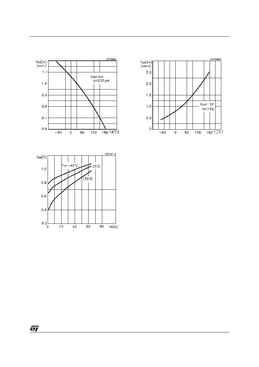
Normalized Gate Threshold Voltage vs
Temperature
Source-drain Diode Forward Characteristics
Normalized On Resistance vs Temperature
STE38NB50F
5/8
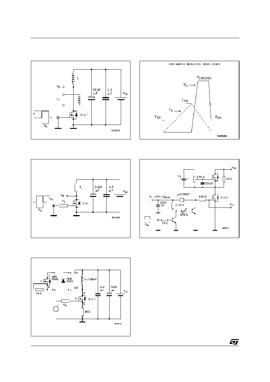
Fig. 1: Unclamped Inductive Load Test Circuit
Fig. 3: Switching Times Test Circuits For
Resistive Load
Fig. 2: Unclamped Inductive Waveform
Fig. 4: Gate Charge test Circuit
Fig. 5: Test Circuit For Inductive Load Switching
And Diode Recovery Times
STE38NB50F
6/8
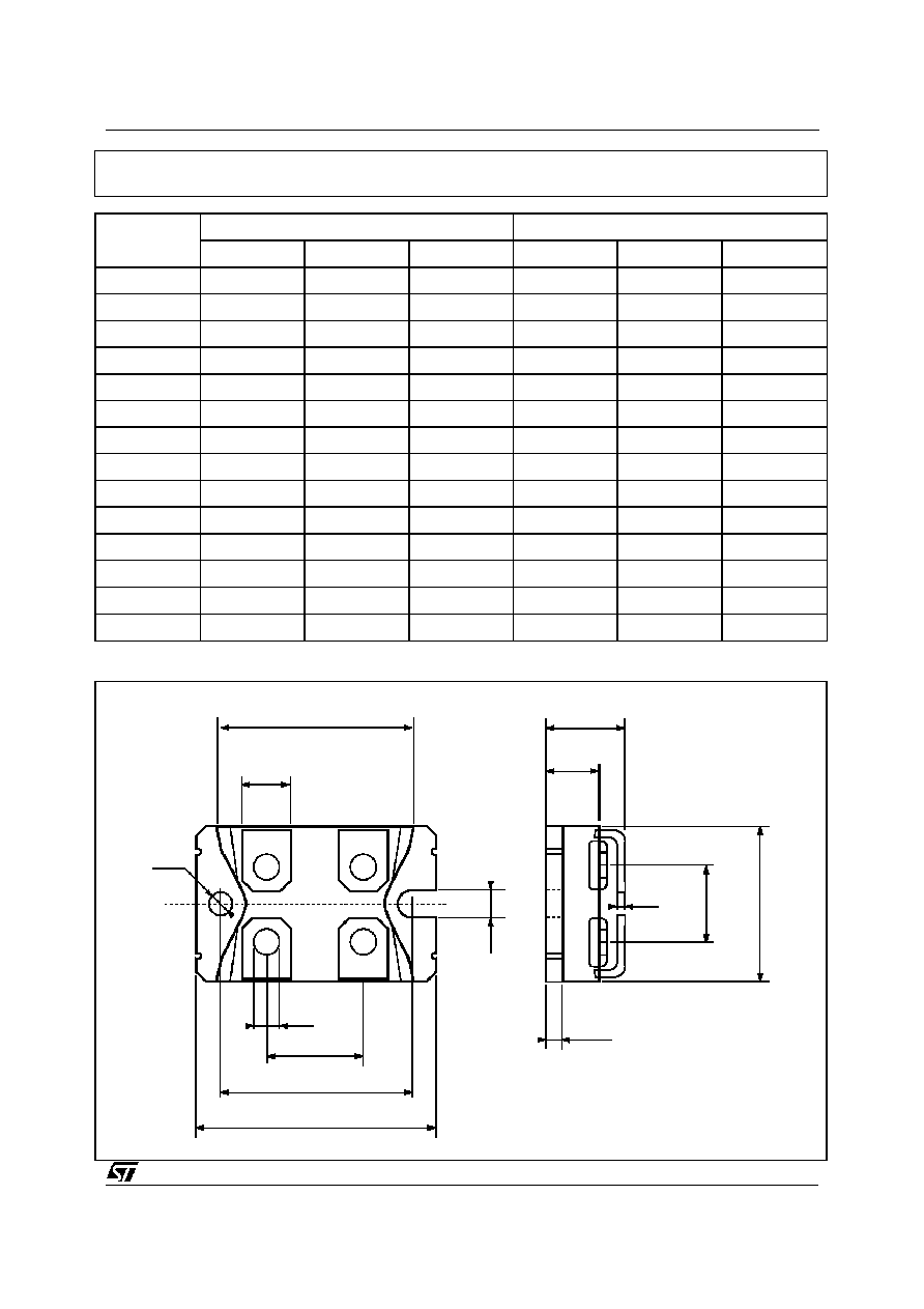
DIM.
mm
inch
MIN.
TYP.
MAX.
MIN.
TYP.
MAX.
A
11.8
12.2
0.466
0.480
B
8.9
9.1
0.350
0.358
C
1.95
2.05
0.076
0.080
D
0.75
0.85
0.029
0.033
E
12.6
12.8
0.496
0.503
F
25.15
25.5
0.990
1.003
G
31.5
31.7
1.240
1.248
H
4
0.157
J
4.1
4.3
0.161
0.169
K
14.9
15.1
0.586
0.594
L
30.1
30.3
1.185
1.193
M
37.8
38.2
1.488
1.503
N
4
0.157
O
7.8
8.2
0.307
0.322
B
E
H
O
N
J
K
L
M
F
A
C
G
D
ISOTOP MECHANICAL DATA
STE38NB50F
7/8

Information furnished is believ ed to be accurate and reliable. However, STMicroelectronics assumes no responsibil ity for the consequences
of use of such information nor for any infringement of patents or other rights of third parties which may result from its use. No license is
granted by implication or otherwise under any patent or patent rights of STMicroelectronics. Specific ation mentioned in this publication are
subjec t to change without notice. This publication supersedes and replaces all information previously supplied. STMicroelectronics products
are not authorized for use as critical components in life support devices or systems without express written approval of STMicroelectronics.
The ST logo is a trademark of STMicroelectronics
©
1999 STMicroelectronics ≠ Printed in Italy ≠ All Rights Reserved
STMicroelectronics GROUP OF COMPANIES
Australia - Brazil - China - Finland - France - Germany - Hong Kong - India - Italy - Japan - Malaysia - Malta - Morocco -
Singapore - Spain - Sweden - Switzerland - United Kingdom - U.S.A.
http://www.st.com
.
STE38NB50F
8/8