 | –≠–ª–µ–∫—Ç—Ä–æ–Ω–Ω—ã–π –∫–æ–º–ø–æ–Ω–µ–Ω—Ç: STE48NM60 | –°–∫–∞—á–∞—Ç—å:  PDF PDF  ZIP ZIP |
1/8
June 2003
STE48NM60
N-CHANNEL 600V - 0.09
- 48A ISOTOP
MDmeshTMPower MOSFET
TYPICAL R
DS
(on) = 0.09
HIGH dv/dt AND AVALANCHE CAPABILITIES
100% AVALANCHE TESTED
LOW INPUT CAPACITANCE AND GATE
CHARGE
LOW GATE INPUT RESISTANCE
TIGHT PROCESS CONTROL AND HIGH
MANUFACTURING YIELDS
DESCRIPTION
The MDmeshTM is a new revolutionary MOSFET
technology that associates the Multiple Drain pro-
cess with the Company's PowerMESHTM horizontal
layout. The resulting product has an outstanding low
on-resistance, impressively high dv/dt and excellent
avalanche characteristics. The adoption of the
Company's proprietary strip technique yields overall
dynamic performance that is significantly better than
that of similar competition's products.
APPLICATIONS
The MDmeshTM family is very suitable for increasing
power density of high voltage converters allowing
system miniaturization and higher efficiencies.
ABSOLUTE MAXIMUM RATINGS
(∑)Pulse width limited by safe operating area
TYPE
V
DSS
R
DS(on)
I
D
STE48NM60
600V
< 0.11
48 A
Symbol
Parameter
Value
Unit
V
DS
Drain-source Voltage (V
GS
= 0)
600
V
V
DGR
Drain-gate Voltage (R
GS
= 20 k
)
600
V
V
GS
Gate- source Voltage
±30
V
I
D
Drain Current (continuous) at T
C
= 25∞C
48
A
I
D
Drain Current (continuous) at T
C
= 100∞C
30
A
I
DM
( )
Drain Current (pulsed)
192
A
P
TOT
Total Dissipation at T
C
= 25∞C
450
W
Derating Factor
3.57
W/∞C
dv/dt (1)
Peak Diode Recovery voltage slope
15
V/ns
T
stg
Storage Temperature
≠65 to 150
∞C
T
j
Max. Operating Junction Temperature
150
∞C
(1) I
SD
48A, di/dt
400A/µs, V
DD
V
(BR)DSS
, T
j
T
JMAX.
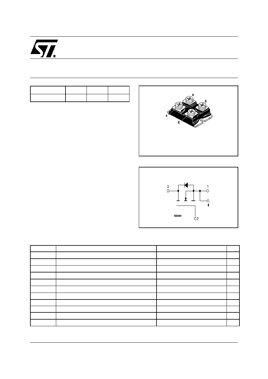
ISOTOP
INTERNAL SCHEMATIC DIAGRAM
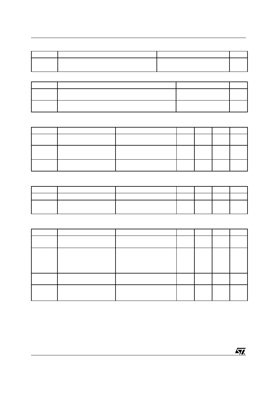
STE48NM60
2/8
THERMAL DATA
AVALANCHE CHARACTERISTICS
ELECTRICAL CHARACTERISTICS (T
CASE
= 25 ∞C UNLESS OTHERWISE SPECIFIED)
OFF
ON (1)
DYNAMIC
1. Pulsed: Pulse duration = 300 µs, duty cycle 1.5 %.
2. C
oss eq.
is defined as a constant equivalent capacitance giving the same charging time as C
oss
when V
DS
increases from 0 to 80%
V
DSS
Rthj-case
Thermal Resistance Junction-case
Max
0.28
∞C/W
Rthj-amb
Thermal Resistance Junction-ambient
Max
30
∞C/W
T
l
Maximum Lead Temperature For Soldering Purpose
300
∞C
Symbol
Parameter
Max Value
Unit
I
AR
Avalanche Current, Repetitive or Not-Repetitive
(pulse width limited by T
j
max)
15
A
E
AS
Single Pulse Avalanche Energy
(starting T
j
= 25 ∞C, I
D
= I
AR
, V
DD
= 35 V)
850
mJ
Symbol
Parameter
Test Conditions
Min.
Typ.
Max.
Unit
V
(BR)DSS
Drain-source
Breakdown Voltage
I
D
= 250 µA, V
GS
= 0
600
V
I
DSS
Zero Gate Voltage
Drain Current (V
GS
= 0)
V
DS
= Max Rating
10
µA
V
DS
= Max Rating, T
C
= 125 ∞C
100
µA
I
GSS
Gate-body Leakage
Current (V
DS
= 0)
V
GS
= ±30V
±100
nA
Symbol
Parameter
Test Conditions
Min.
Typ.
Max.
Unit
V
GS(th)
Gate Threshold Voltage
V
DS
= V
GS
, I
D
= 250µA
3
4
5
V
R
DS(on)
Static Drain-source On
Resistance
V
GS
= 10V, I
D
= 22.5A
0.09
0.11
Symbol
Parameter
Test Conditions
Min.
Typ.
Max.
Unit
g
fs
(1)
Forward Transconductance
V
DS
> I
D(on)
x R
DS(on)max,
I
D
= 22.5A
15
S
C
iss
Input Capacitance
V
DS
= 25V, f = 1 MHz, V
GS
= 0
3800
pF
C
oss
Output Capacitance
1250
pF
C
rss
Reverse Transfer
Capacitance
46
pF
C
oss eq.
(2)
Equivalent Output
Capacitance
V
GS
= 0V, V
DS
= 0V to 480V
340
pF
R
G
Gate Input Resistance
f=1 MHz Gate DC Bias = 0
Test Signal Level = 20mV
Open Drain
1.4
3/8
STE48NM60
ELECTRICAL CHARACTERISTICS (CONTINUED)
SWITCHING ON
SWITCHING OFF
SOURCE DRAIN DIODE
Note: 1. Pulsed: Pulse duration = 300 µs, duty cycle 1.5 %.
2. Pulse width limited by safe operating area.
Symbol
Parameter
Test Conditions
Min.
Typ.
Max.
Unit
t
d(on)
Turn-on Delay Time
V
DD
= 250V, I
D
= 22.5A
R
G
= 4.7
V
GS
= 10V
(see test circuit, Figure 3)
30
ns
t
r
Rise Time
20
ns
Q
g
Total Gate Charge
V
DD
= 400V, I
D
= 45A,
V
GS
= 10V
96
134
nC
Q
gs
Gate-Source Charge
31
nC
Q
gd
Gate-Drain Charge
43
nC
Symbol
Parameter
Test Conditions
Min.
Typ.
Max.
Unit
t
r(Voff)
Off-voltage Rise Time
V
DD
= 400V, I
D
= 45A,
R
G
= 4.7
,
V
GS
= 10V
(see test circuit, Figure 5)
16
ns
t
f
Fall Time
23
ns
t
c
Cross-over Time
40
ns
Symbol
Parameter
Test Conditions
Min.
Typ.
Max.
Unit
I
SD
Source-drain Current
48
A
I
SDM
(2)
Source-drain Current (pulsed)
192
A
V
SD
(1)
Forward On Voltage
I
SD
= 45A, V
GS
= 0
1.5
V
t
rr
Q
rr
I
RRM
Reverse Recovery Time
Reverse Recovery Charge
Reverse Recovery Current
I
SD
= 45A, di/dt = 100A/µs,
V
DD
= 100 V, T
j
= 25∞C
(see test circuit, Figure 5)
508
10
40
ns
µC
A
t
rr
Q
rr
I
RRM
Reverse Recovery Time
Reverse Recovery Charge
Reverse Recovery Current
I
SD
= 45A, di/dt = 100A/µs,
V
DD
= 100 V, T
j
= 150∞C
(see test circuit, Figure 5)
650
14
43
ns
µC
A
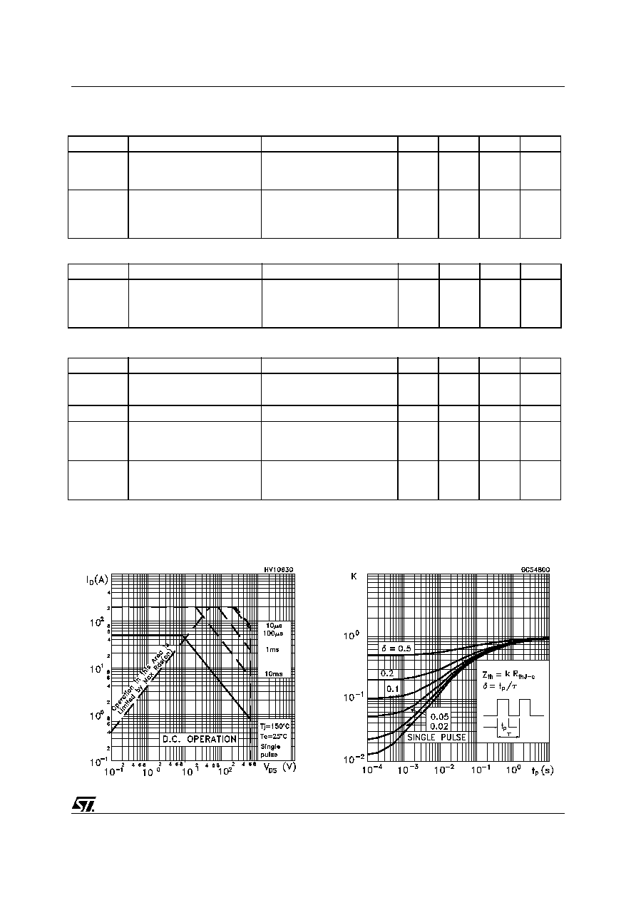
Safe Operating Area
Thermal Impedance
STE48NM60
4/8
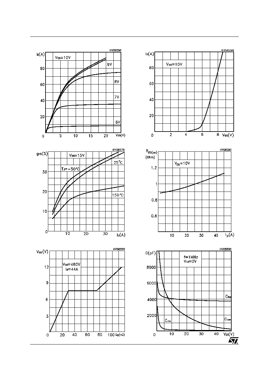
Gate Charge vs Gate-source Voltage
Capacitance Variations
Transconductance
Static Drain-source On Resistance
Output Characteristics
Transfer Characteristics
5/8
STE48NM60
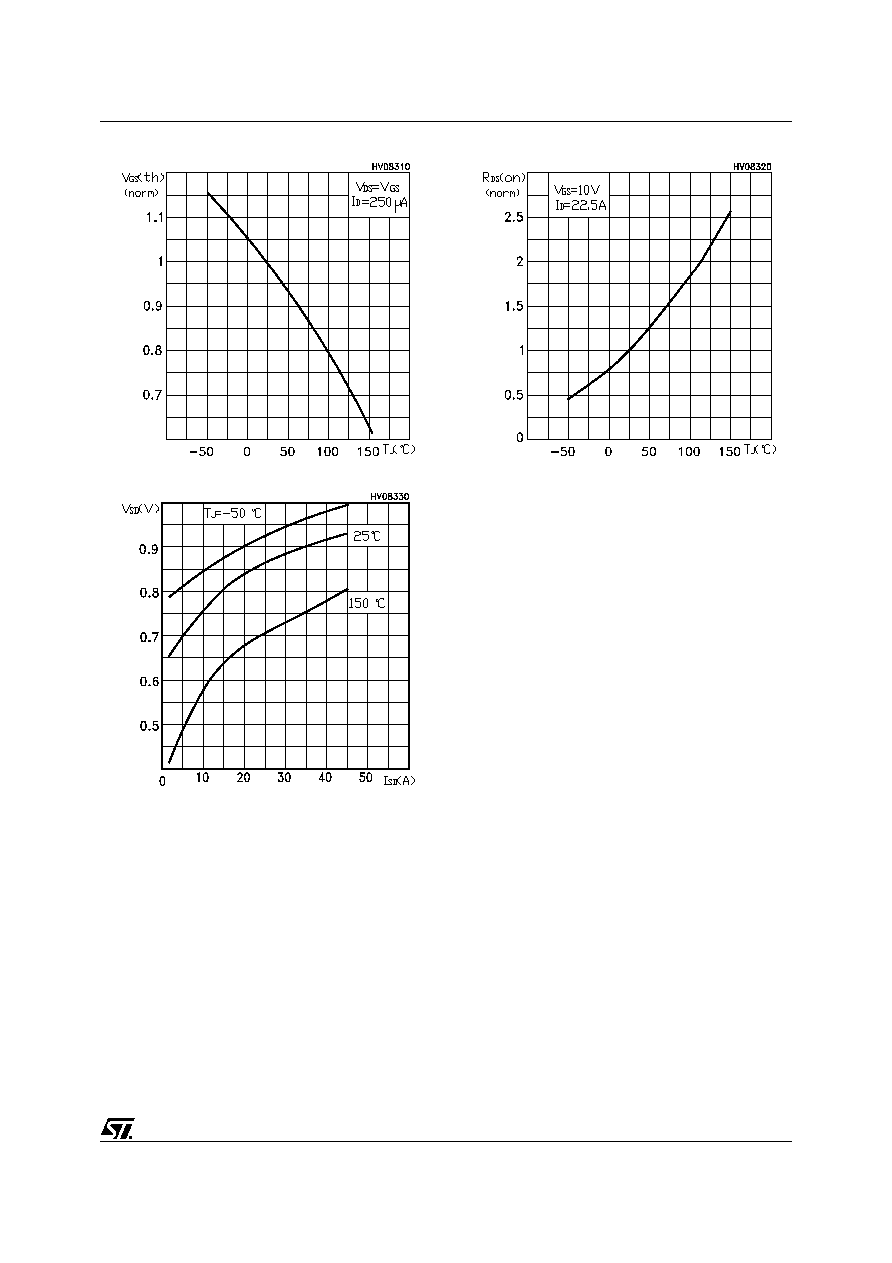
Source-drain Diode Forward Characteristics
Normalized On Resistance vs Temperature
Normalized Gate Thereshold Voltage vs Temp.
STE48NM60
6/8
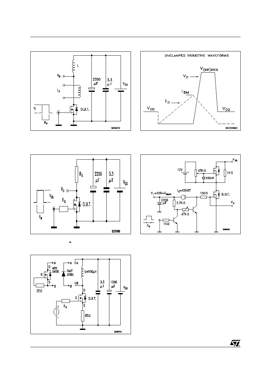
Fig. 5: Test Circuit For Inductive Load Switching
And Diode Recovery Times
Fig. 4: Gate Charge test Circuit
Fig. 2: Unclamped Inductive Waveform
Fig. 1: Unclamped Inductive Load Test Circuit
Fig. 3: Switching Times Test Circuit For
Resistive Load
7/8
STE48NM60
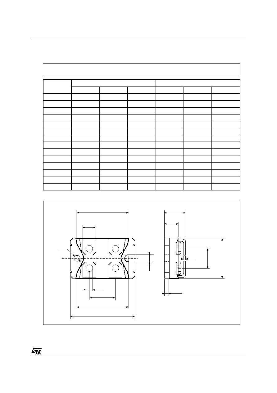
DIM.
mm
inch
MIN.
TYP.
MAX.
MIN.
TYP.
MAX.
A
11.8
12.2
0.466
0.480
B
8.9
9.1
0.350
0.358
C
1.95
2.05
0.076
0.080
D
0.75
0.85
0.029
0.033
E
12.6
12.8
0.496
0.503
F
25.15
25.5
0.990
1.003
G
31.5
31.7
1.240
1.248
H
4
0.157
J
4.1
4.3
0.161
0.169
K
14.9
15.1
0.586
0.594
L
30.1
30.3
1.185
1.193
M
37.8
38.2
1.488
1.503
N
4
0.157
O
7.8
8.2
0.307
0.322
B
E
H
O
N
J
K
L
M
F
A
C
G
D
ISOTOP MECHANICAL DATA

STE48NM60
8/8
Information furnished is believed to be accurate and reliable. However, STMicroelectronics assumes no responsibility for the
consequences of use of such information nor for any infringement of patents or other rights of third parties which may result from
its use. No license is granted by implication or otherwise under any patent or patent rights of STMicroelectronics. Specifications
mentioned in this publication are subject to change without notice. This publication supersedes and replaces all information
previously supplied. STMicroelectronics products are not authorized for use as critical components in life support devices or
systems without express written approval of STMicroelectronics.
© The ST logo is a registered trademark of STMicroelectronics
© 2003 STMicroelectronics - Printed in Italy - All Rights Reserved
STMicroelectronics GROUP OF COMPANIES
Australia - Brazil - Canada - China - Finland - France - Germany - Hong Kong - India - Israel - Italy - Japan - Malaysia - Malta - Morocco
Singapore - Spain - Sweden - Switzerland - United Kingdom - United States.
© http://www.st.com