128-BIT 3D MULTIMEDIA ACCELERATOR
PRELIMINARY DATA
Æ
RIVA 128ZX
TM
1/85
The information in this datasheet is subject to change
7071857 00
June 1998
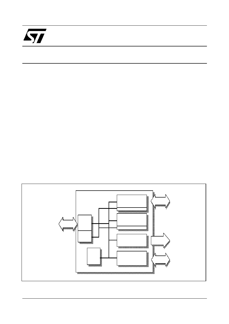
BLOCK DIAGRAM
Palette DAC
YUV - RGB,
Graphics Engine
128 bit 2D
Direct3D
8MByte
VGA
DMA Bus
Internal
Bus
CCIR656
Video
PCI/AGP
128 bit
interface
Monitor/
TV
1.6 GByte/s
Internal Bus
Bandwidth
DMA Engine
Video Port
X & Y scaler
Host
Interface
FIFO/
DMA
Pusher
DMA Engine
SDRAM/SGRAM
Interface
KEY FEATURES
∑
Fast 32-bit VGA/SVGA
∑
High performance 128-bit 2D/GUI/DirectDraw
Acceleration
∑
Interactive, Photorealistic Direct3D Accelera-
tion with advanced effects
∑
Pinout backwards compatible with RIVA 128
∑
Massive 1.6Gbytes/s, 100MHz 128-bit wide
8MByte SGRAM framebuffer interface
∑
Adds 16Mbit SDRAM support for cost sensitive
8MByte framebuffer applications
∑
Video Acceleration for DirectDraw/DirectVideo,
MPEG-1/2 and Indeo
Æ
- Planar 4:2:0 and packed 4:2:2 Color Space
Conversion
- X and Y smooth up and down scaling
∑
250MHz
Palette-DAC
supporting
up
to
1600x1200@85Hz
∑
NTSC and PAL output with flicker-filter
∑
Multi-function Video Port and serial interface
∑
Bus mastering DMA Accelerated Graphics Port
(AGP) 1.0 Interface supporting 133MHz 2X
data transfer mode
∑
Bus mastering DMA PCI 2.1 interface
∑
ACPI power management interface support
∑
0.35 micron 5LM CMOS
∑
300 PBGA
DESCRIPTION
The RIVA128ZX
TM
offers unparalleled 2D and 3D
performance, meeting all the requirements of the
mainstream PC graphics market and Microsoft's
PC'97. RIVA128ZX combines all the features of
RIVA 128 plus 8MByte SDRAM and SGRAM
based framestore support and AGP 2X data trans-
fer. It provides the most advanced Direct3D
TM
ac-
celeration solution and delivers leadership VGA,
2D and Video performance, enabling a range of
applications from 3D games through to DVD, In-
tercast
TM
and video conferencing.

RIVA128ZX
128-BIT 3D MULTIMEDIA ACCELERATOR
TABLE OF CONTENTS
2/85
1
RIVA128ZX 300PBGA DEVICE PINOUT.......................................................................................
4
2
PIN DESCRIPTIONS ......................................................................................................................
5
2.1
ACCELERATED GRAPHICS PORT (AGP) INTERFACE .....................................................
5
2.2
PCI 2.1 LOCAL BUS INTERFACE ........................................................................................
5
2.3
FRAMEBUFFER INTERFACE ..............................................................................................
7
2.4
VIDEO PORT.........................................................................................................................
7
2.5
DEVICE ENABLE SIGNALS ..................................................................................................
8
2.6
DISPLAY INTERFACE ..........................................................................................................
8
2.7
VIDEO DAC AND PLL ANALOG SIGNALS ..........................................................................
8
2.8
POWER SUPPLY ..................................................................................................................
8
2.9
TEST......................................................................................................................................
9
3
OVERVIEW OF THE RIVA128ZX ..................................................................................................
10
3.1
BALANCED PC SYSTEM ......................................................................................................
10
3.2
HOST INTERFACE ...............................................................................................................
10
3.3
2D ACCELERATION .............................................................................................................
11
3.4
3D ENGINE ...........................................................................................................................
11
3.5
VIDEO PROCESSOR ............................................................................................................
11
3.6
VIDEO PORT.........................................................................................................................
12
3.7
DIRECT RGB OUTPUT TO LOW COST PAL/NTSC ENCODER .........................................
12
3.8
SUPPORT FOR STANDARDS..............................................................................................
12
3.9
RESOLUTIONS SUPPORTED..............................................................................................
12
3.10 CUSTOMER EVALUATION KIT ............................................................................................
13
3.11 TURNKEY MANUFACTURING PACKAGE ...........................................................................
13
4
ACCELERATED GRAPHICS PORT (AGP) INTERFACE .............................................................
14
4.1
RIVA128ZX AGP INTERFACE ..............................................................................................
15
4.2
AGP BUS TRANSACTIONS..................................................................................................
15
5
PCI 2.1 LOCAL BUS INTERFACE.................................................................................................
23
5.1
RIVA128ZX PCI INTERFACE ...............................................................................................
23
5.2
PCI TIMING SPECIFICATION ...............................................................................................
24
6
FRAMEBUFFER INTERFACE .......................................................................................................
30
6.1
SDRAM INTERFACE ............................................................................................................
31
6.2
SGRAM INTERFACE ............................................................................................................
32
6.3
SDRAM/SGRAM ACCESSES AND COMMANDS ................................................................
35
6.4
LAYOUT OF FRAMEBUFFER CLOCK SIGNALS ................................................................
37
6.5
FRAMEBUFFER INTERFACE TIMING SPECIFICATION ....................................................
37
7
VIDEO PLAYBACK ARCHITECTURE...........................................................................................
42
7.1
VIDEO SCALER PIPELINE ...................................................................................................
43
8
VIDEO PORT ..................................................................................................................................
45
8.1
VIDEO INTERFACE PORT FEATURES ...............................................................................
45
8.2
BI-DIRECTIONAL MEDIA PORT POLLING COMMANDS USING MPC ..............................
46
8.3
TIMING DIAGRAMS ..............................................................................................................
47
8.4
656 MASTER MODE .............................................................................................................
51
8.5
VBI HANDLING IN THE VIDEO PORT .................................................................................
52
8.6
SCALING IN THE VIDEO PORT ...........................................................................................
52
9
BOOT ROM INTERFACE...............................................................................................................
53

128-BIT 3D MULTIMEDIA ACCELERATOR
RIVA128ZX
3/85
10
POWER-ON RESET CONFIGURATION........................................................................................
55
11
DISPLAY INTERFACE ...................................................................................................................
57
11.1 PALETTE-DAC ......................................................................................................................
57
11.2 PIXEL MODES SUPPORTED ...............................................................................................
57
11.3 HARDWARE CURSOR .........................................................................................................
58
11.4 SERIAL INTERFACE.............................................................................................................
59
11.5 ANALOG INTERFACE ..........................................................................................................
60
11.6 TV OUTPUT SUPPORT ........................................................................................................
61
12
IN-CIRCUIT BOARD TESTING ......................................................................................................
63
12.1 TEST MODES .......................................................................................................................
63
12.2 CHECKSUM TEST ................................................................................................................
63
13
ELECTRICAL SPECIFICATIONS ..................................................................................................
64
13.1 ABSOLUTE MAXIMUM RATINGS ........................................................................................
64
13.2 OPERATING CONDITIONS ..................................................................................................
64
13.3 DC SPECIFICATIONS...........................................................................................................
64
13.4 ELECTRICAL SPECIFICATIONS ..........................................................................................
65
13.5 DAC CHARACTERISTICS ....................................................................................................
65
13.6 FREQUENCY SYNTHESIS CHARACTERISTICS ................................................................
66
14
PACKAGE DIMENSION SPECIFICATION ....................................................................................
67
14.1 300 PIN BALL GRID ARRAY PACKAGE ..............................................................................
67
15
REFERENCES................................................................................................................................
68
16
ORDERING INFORMATION ..........................................................................................................
68
APPENDIX ...............................................................................................................................................
69
A
PCI CONFIGURATION REGISTERS .............................................................................................
69
A.1
REGISTER DESCRIPTIONS FOR PCI CONFIGURATION SPACE ....................................
69
128-BIT 3D MULTIMEDIA ACCELERATOR
RIVA128ZX
4/85
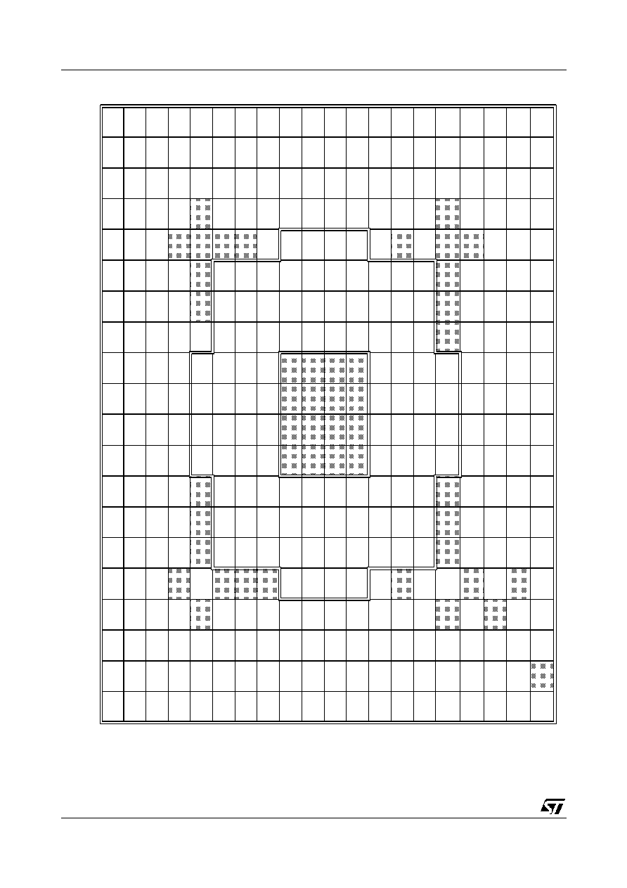
1
RIVA128ZX 300PBGA DEVICE PINOUT
NOTES
1
NIC = No Internal Connection. Do not connect to these pins.
2
VDD=3.3V
Signals denoted with an asterisk are defined for future expansion. See
Pin Descriptions, Section 2, page 5 for details.
12345
6789
1
0
1
1
1
2
1
3
1
4
1
5
1
6
1
7
1
8
1
9
2
0
A
FBD[4]
FBD[6]
FBD[7]
FBD[17]
FBD[19]
FBD[21]
FBD[23]
FBDQM[2]
FBA[0]
FBA[2]
FBA[4]
FBA[6]
FBA[8]
FBDQM[5]
FBD[41]
FBD[43]
FBD[45]
FBD[47]
FBD[56]
FBD[57]
B
FBD[3]
FBD[5]
FBD[16]
FBD[18]
FBD[20]
FBD[22]
FBDQM[0]
FBA[9]
FBA[1]
FBA[3]
FBA[5]
FBA[7]
FBCLK1
FBDQM[7]
FBD[40]
FBD[42]
FBD[44]
FBD[46]
FBD[58]
FBD[59]
C
FBD[1]
FBD[2]
FBD[28]
FBD[27]
FBD[26]
FBD[25]
FBD[15]
FBD[13]
FBD[11]
FBD[9]
FBDQM[1]
FBWE#
FBRAS#
FBA[10]
FBDQM[4]
FBD[55]
FBD[54]
FBD[53]
FBD[6
0]
FBD[61]
D
FBCLK0
FBD[0]
FBD[29]
FBD[30]
VDD
FBD[24]
FBD[14]
FBD[12]
FBD[10]
FBD[8]
FBDQM[3]
FBCAS#
FBCS0
FBCS1
FBDQM[6]
VDD
FBD[52]
FBD[51]
FBD[62]
FBD[63]
E
SCL
FBCLK2
FBD[31]
VDD
NIC
VDD
VDD
VDD
FBCKE
VDD
VDD
VDD
VDD
FBD[50]
FBD[39]
FBD[38]
F
MP_AD[6]
NIC
SDA
FBCLKFB
VDD
VDD
FBD[48]
FBD[49]
FBD[37]
FBD[36]
G
MPFRAME#
MP_AD[7]
MP_AD[5]
MP_AD[4]
MPCLAMP
VDD
FBD[35]
FBD[34]
FBD[33]
FBD[32]
H
MP_AD[2]
MPSTOP#
MPCLK
MP_AD[3]
VDD
NIC
FBDQM[12]
FBDQM[14]
FBDQM[15]
FBDQM[13]
J
FBDQM[8]
MPDTACK#
MP_AD[1]
MP_AD[0]
GND
GND
GND
GND
FBD[118]
FBD[119]
FBD[105]
FBD[104]
K
FBDQM[9]
FBD[87]
FBDQM[10]
FBDQM[11]
GND
GND
GND
GND
FBD[116]
FBD[117]
FBD[107]
FBD[106]
L
FBD[86]
FBD[85]
FBD[72]
FBD[73]
GND
GND
GND
GND
FBD[114]
FBD[115]
FBD[109]
FBD[108]
M
FBD[84]
FBD[83]
FBD[74]
FBD[75]
GND
GND
GND
GND
FBD[112]
FBD[113]
FBD[111]
FBD[110]
N
FBD[82]
FBD[81]
FBD[76]
FBD[77]
NIC
NIC
FBD[102]
FBD[103]
FBD[121]
FBD[120]
P
FBD[80]
FBD[71]
FBD[78]
FBD[79]
VDD
VDD
FBD[100]
FBD[101]
FBD[123]
FBD[122]
R
FBD[70]
FBD[69]
FBD[88]
FBD[89]
NIC
NIC
FBD[98]
FBD[99]
FBD[125]
FBD[124]
T
FBD[68]
FBD[67]
FBD[90]
VDD
NIC
HOSTVDD
HOSTVDD
HOST-
CLAMP
HOSTVDD
HOST-
CLAMP
HOSTVDD
HOST-
CLAMP
VDD
FBD[97]
FBD[127]
FBD[126]
U
FBD[66]
FBD[65]
FBD[92]
FBD[91]
HOST-
CLAMP
XTALOUT
PCIRST#
AGPST[1]
PCIAD[30]
PCIAD[26]
PCICBE#[3]
PCIAD[20]
PCIAD[16]
PCITRDY#
PCIPAR
HOSTVDD
PCICBE#[0]
FBD[96]
VIDVSYNC
VIDHSYNC
V
FBD[64]
FBD[95]
RED
DACVDD
VREF
PCIINTA#
PCIGNT#
AGPPIPE#
PCIAD[28]
PCIAD[24]
PCIAD[22]
PCIAD[18]
PCIFRAME#
PCISTOP#
PCIAD[15]
PCIAD[11]
PCIAD[
6]
PCIAD[2]
TESTMODE
ROMCS#
W
FBD[93]
FBD[94]
BLUE
COMP
PLLVDD
PCIREQ#
AGPST[2]
PCIAD[31]
PCIAD[27]
AGPAD-
STB1
PCIAD[21]
PCIAD[17]
PCIIRDY#
PCICBE#[1]
PCIAD[13]
PCIAD[9]
PCIAD[4]
PCIAD[0]
PCIAD[7]
PCIAD[5]
Y
GREEN
GND
RSET
XTALIN
PCICLK
AGPST[0]
PCIIDSEL/
AGPRBF#
PCIAD[29]
PCIAD[25]
PCIAD[23]
PCIAD[19]
PCICBE#[2]
PCI-
DEVSEL#
PCIAD[14]
PCIAD[12]
PCIAD[10]
PCIAD[8]
AGPAD-
STB0
PCIAD[3]
PCIAD[1]
128-BIT 3D MULTIMEDIA ACCELERATOR
RIVA128ZX
5/85
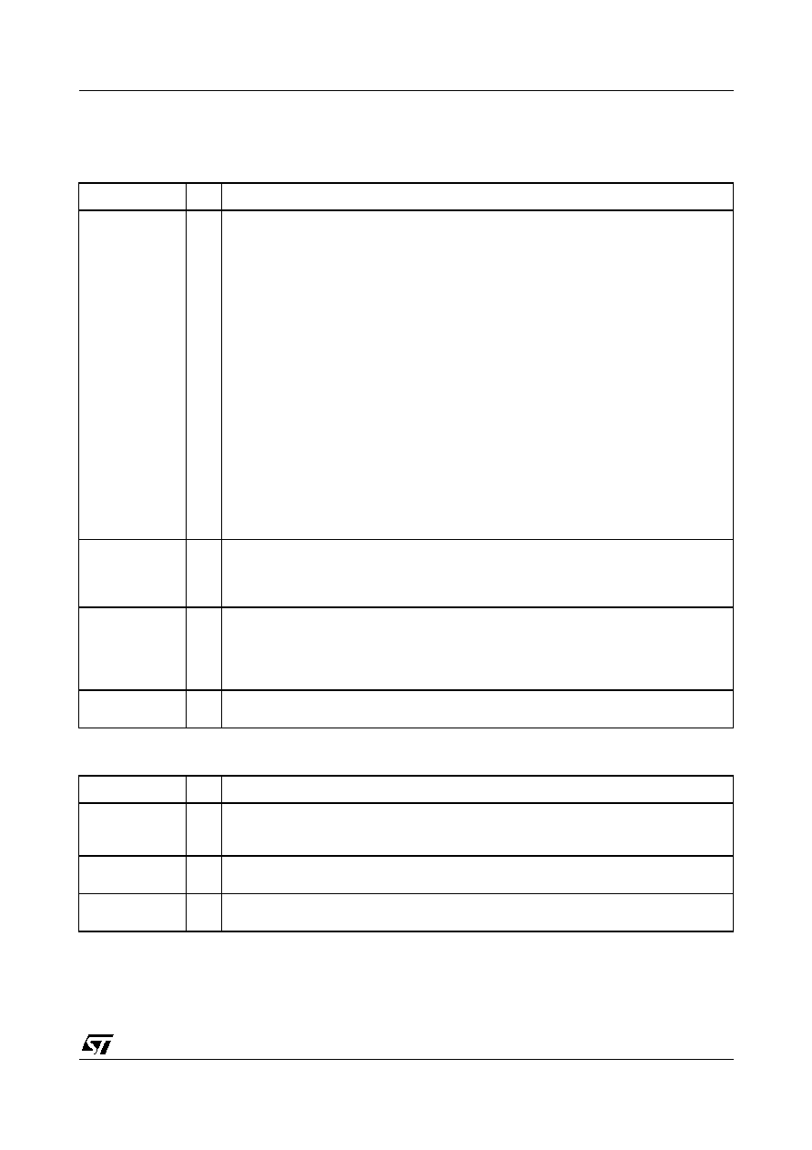
2
PIN DESCRIPTIONS
2.1
ACCELERATED GRAPHICS PORT (AGP) INTERFACE
2.2
PCI 2.1 LOCAL BUS INTERFACE
Signal
I/O
Description
AGPST[2:0]
I
AGP status bus providing information from the arbiter to the RIVA128ZX on what it may
do. AGPST[2:0] only have meaning to the RIVA128ZX when PCIGNT# is asserted. When
PCIGNT# is de-asserted these signals have no meaning and must be ignored.
000
Indicates that previously requested low priority read or flush data is being
returned to the RIVA128ZX.
001
Indicates that previously requested high priority read data is being returned to
the RIVA128ZX.
010
Indicates that the RIVA128ZX is to provide low priority write data for a previous
enqueued write command.
011
Indicates that the RIVA128ZX is to provide high priority write data for a previous
enqueued write command.
100
Reserved
101
Reserved
110
Reserved
111
Indicates that the RIVA128ZX has been given permission to start a bus transac-
tion. The RIVA128ZX may enqueue AGP requests by asserting AGPPIPE# or
start a PCI transaction by asserting PCIFRAME#. AGPST[2:0] are always an
output from the Core Logic (AGP chipset) and an input to the RIVA128ZX.
AGPRBF#
O
Read Buffer Full indicates when the RIVA128ZX is ready to accept previously requested
low priority read data or not. When AGPRBF# is asserted the arbiter is not allowed to
return (low priority) read data to the RIVA128ZX. This signal should be pulled up via a
4.7K
resistor (although it is supposed to be pulled up by the motherboard chipset).
AGPPIPE#
O
Pipelined Read is asserted by RIVA128ZX (when the current master) to indicate a full
width read address is to be enqueued by the target. The RIVA128ZX enqueues one
request each rising clock edge while AGPPIPE# is asserted. When AGPPIPE# is de-
asserted no new requests are enqueued across PCIAD[31:0]. AGPPIPE# is a sustained
tri-state signal from the RIVA128ZX and is an input to the target (the core logic).
AGPADSTB0
,
AGPADSTB1
I/O
Bus strobe signals providing timing for AGP 2X data transfer mode on PCIAD[15:00] and
PCIAD[31:16] respectively. The agent that is supplying data drives these signals.
Signal
I/O
Description
PCICLK
I
PCI clock. This signal provides timing for all transactions on the PCI bus, except for
PCIRST# and PCIINTA#. All PCI signals are sampled on the rising edge of PCICLK and
all timing parameters are defined with respect to this edge .
PCIRST#
I
PCI reset. This signal is used to bring registers, sequencers and signals to a consistent
state. When PCIRST# is asserted all output signals are tristated.
PCIAD[31:0]
I/O
32-bit multiplexed address and data bus. A bus transaction consists of an address phase
followed by one or more data phases.