 | ÐлекÑÑоннÑй компоненÑ: STG3699 | СкаÑаÑÑ:  PDF PDF  ZIP ZIP |
Äîêóìåíòàöèÿ è îïèñàíèÿ www.docs.chipfind.ru
1/12
May 2004
s
HIGH SPEED:
t
PD
= 0.3ns (TYP.) at V
CC
= 3.0V
t
PD
= 0.4ns (TYP.) at V
CC
= 2.3V
s
ULTRA LOW POWER DISSIPATION:
I
CC
= 0.2
µ
A (MAX.) at T
A
= 85°C
s
LOW "ON" RESISTANCE V
IN
=0V:
R
ON
= 0.5
(MAX. T
A
= 25°C) at V
CC
= 2.7V
R
ON
= 0.8
(MAX. T
A
= 25°C) at V
CC
= 2.3V
R
ON
= 3.0
(MAX. T
A
= 25°C) at V
CC
= 1.8V
s
WIDE OPERATING VOLTAGE RANGE:
V
CC
(OPR) = 1.65V to 4.3V SINGLE SUPPLY
s
4.3V TOLERANT AND 1.8V COMPATIBLE
THRESHOLD ON DIGITAL CONTROL INPUT
at V
CC
= 2.3 to 3.0V
s
LATCH-UP PERFORMANCE EXCEEDS
300mA (JESD 17)
DESCRIPTION
The STG3699 is an high-speed CMOS LOW
VOLTAGE QUAD ANALOG S.P.D.T. (Single Pole
Dual
Throw)
SWITCH
or
2:1
Multiplexer/
Demultiplexer Switch fabricated in silicon gate
C
2
MOS technology. It is designed to operate from
1.65V to 4.3V, making this device ideal for
portable applications.
It offers very low ON-Resistance (<0.5
) at
V
CC
=3.0V. The nIN inputs are provided to control
the switches. The switches nS1 are ON (they are
connected to common Ports Dn) when the nIN
input is held high and OFF (high impedance state
exists between the two ports) when nIN is held
low; the switches nS2 are ON (they are connected
to common Ports Dn) when the nIN input is held
low and OFF (high impedance state exists
between the two ports) when IN is held high.
Additional key features are fast switching speed,
Break Before Make Delay Time and Ultra Low
Power Consumption. All inputs and outputs are
equipped with protection circuits against static
discharge,
giving
them
ESD
immunity
and
transient excess voltage. It's available in the
commercial temperature range in TSSOP and
QFN3x3mm package.
STG3699
LOW VOLTAGE 0.5
MAX QUAD SPDT SWITCH
WITH BREAK BEFORE MAKE FEATURE
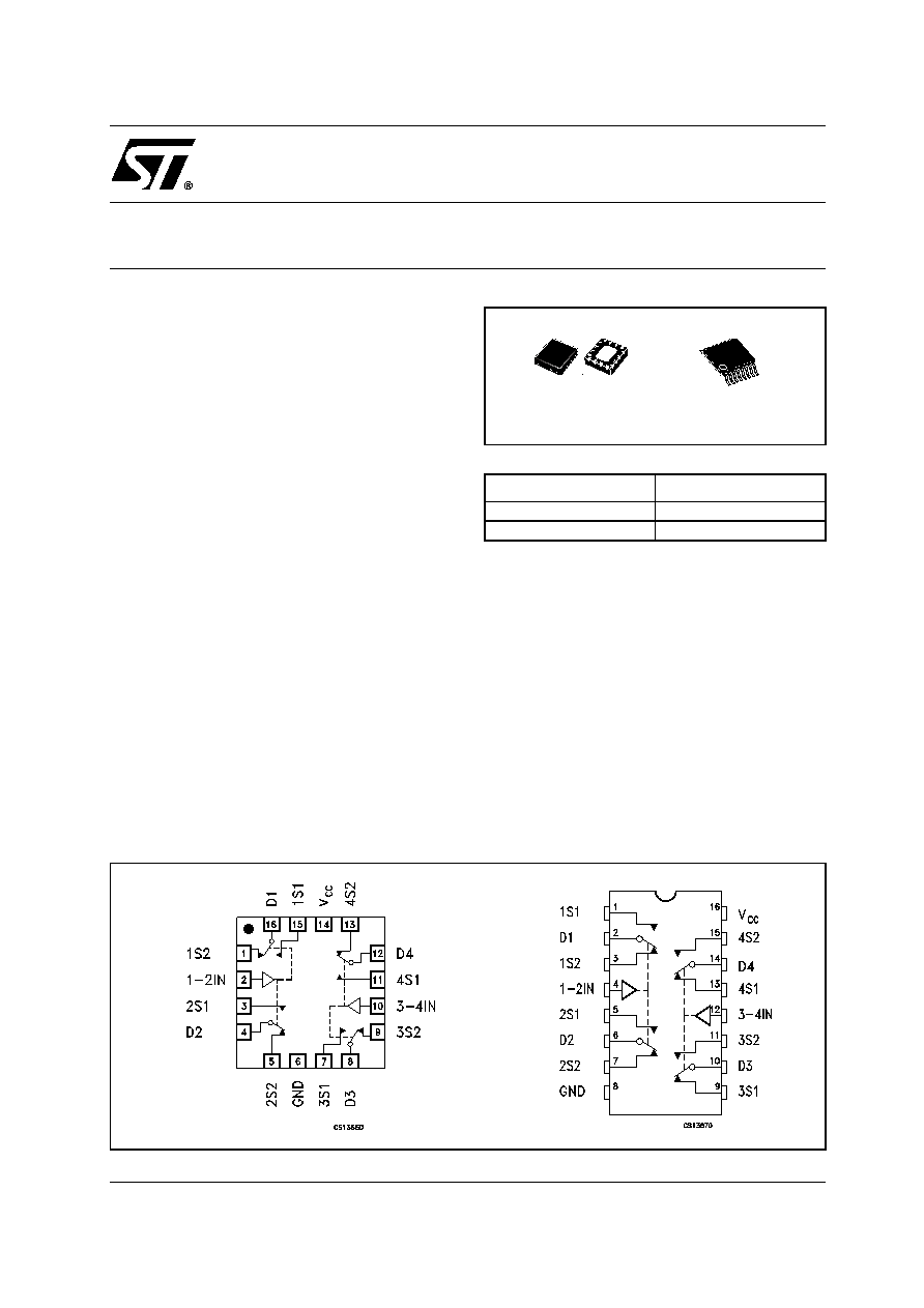
PIN CONNECTION
ORDER CODES
PACKAGE
T & R
TSSOP
STG3699TTR
QFN
STG3699QTR
QFN
TSSOP
Rev. 3
STG3699
2/12
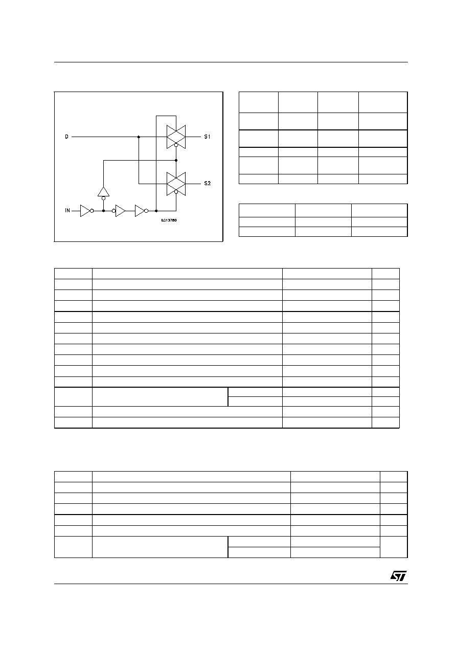
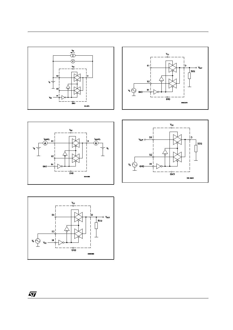
Figure 1: Input Equivalent Circuit
Table 1: Pin Description
Table 2: Truth Table
(*) High Impedance
Table 3: Absolute Maximum Ratings
Absolute Maximum Ratings are those values beyond which damage to the device may occur. Functional operation under these conditions
not implied.
(1) Derate above 70°C: by 18.5mW/°C for QFN package; by 5.6mW/°C for TSSOP.
Table 4: Recommended Operating Conditions
1) Truth Table guaranteed: 1.2V to 4.3V.
TSSOP
PIN N°
QFN
PIN N°
SYMBOL
NAME AND
FUNCTION
1, 5, 9, 13,
3, 7, 11, 15
15, 3, 7, 11,
1, 5, 9, 13
1S1 to 4S1,
1S2 to 4S2
Independent
Channels
2, 6, 10, 14 16, 4, 8, 12
D1 to D4
Common
Channels
4, 12
2, 10
1-2IN, 3-4IN Controls
16
14
V
CC
Positive Sup-
ply Voltage
8
6
GND
Ground (0V)
IN
SWITCH S1
SWITCH S2
H
ON
OFF(*)
L
OFF(*)
ON
Symbol
Parameter
Value
Unit
V
CC
Supply Voltage
-0.5 to 4.6
V
V
I
DC Input Voltage
-0.5 to V
CC
+ 0.5
V
V
IC
DC Control Input Voltage
-0.5 to 4.6
V
V
O
DC Output Voltage
-0.5 to V
CC
+ 0.5
V
I
IKC
DC Input Diode Current on control pin (V
IN
< 0V)
-
50
mA
I
IK
DC Input Diode Current (V
IN
< 0V)
±
50
mA
I
OK
DC Output Diode Current
±
20
mA
I
O
DC Output Current
±
300
mA
I
OP
DC Output Current Peak (pulse at 1ms, 10% duty cycle)
±
500
mA
I
CC
or I
GND
DC V
CC
or Ground Current
±
100
mA
P
D
Power Dissipation at T
a
=70°C (1)
QFN
1120
mW
TSSOP
500
mW
T
stg
Storage Temperature
-65 to 150
°C
T
L
Lead Temperature (10 sec)
300
°C
Symbol
Parameter
Value
Unit
V
CC
Supply Voltage (note 1)
1.65 to 4.3
V
V
I
Input Voltage
0 to V
CC
V
V
IC
Control Input Voltage
0 to 4.3
V
V
O
Output Voltage
0 to V
CC
V
T
op
Operating Temperature
-55 to 125
°C
dt/dv
Input Rise and Fall Time Control Input
V
CC
= 1.65V to 2.7V
0 to 20
ns/V
V
CC
= 3.0V to 4.3V
0 to 10
STG3699
3/12
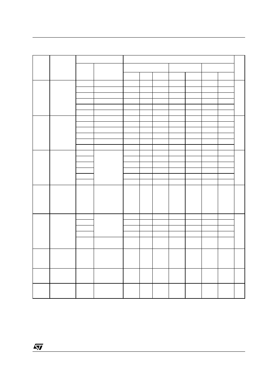
Table 5: DC Specifications
Note 1: Guaranteed by design
Note 2:
R
ON
= R
ON(MAX)
- R
ON(MIN)
.
Note 3: Flatness is defined as the difference between the maximum and minimum value of on-resistance as measured over the specified
analog signal ranges.
Symbol
Parameter
Test Conditions
Value
Unit
V
CC
(V)
T
A
= 25°C
-40 to 85°C
-55 to 125°C
Min.
Typ.
Max.
Min.
Max.
Min.
Max.
V
IH
High Level
Input Voltage
1.65-1.95
0.65V
CC
0.65V
CC
0.65V
CC
V
2.3-2.5
1.4
1.4
1.4
2.7-3.0
1.4
1.4
1.4
3.3
1.5
1.5
1.5
3.6
1.7
1.7
1.7
4.3
2.2
2.2
2.2
V
IL
Low Level
Input Voltage
1.65-1.95
0.40
0.40
0.40
V
2.3-2.5
0.50
0.50
0.50
2.7-3.0
0.50
0.50
0.50
3.3
0.50
0.50
0.50
3.6
0.50
0.50
0.50
4.3
1.3
1.3
1.3
R
ON
Switch ON
Resistance
(1)
4.3
V
S
=0V to V
CC
I
S
=100mA
0.40
0.50
0.60
3.0
0.40
0.50
0.60
2.7
0.40
0.50
0.60
2.3
0.50
0.80
0.80
1.8
0.70
3.0
4.0
1.65
0.80
3.0
4.0
R
ON
ON
Resistance
Match
between
channels
(1,2)
2.7
V
S
=1.5V
I
S
=100mA
0.06
R
FLAT
ON
Resistance
FLATNESS
(3)
4.3
V
S
=1.5V
I
S
=100mA
3.0
2.7
0.07
0.15
0.15
2.3
1.65
V
S
=0.8V
I
S
=100mA
I
OFF
OFF State
Leakage
Current
(nSn), (Dn)
4.3
V
S
=0.3 or 4V
±
10
±
100
nA
I
IN
Input
Leakage
Current
0 - 4.3
V
IN
= 0 to 4.3V
±
0.1
±
1
µ
A
I
CC
Quiescent
Supply
Current (1)
1.65-4.3
V
IN
=V
CC
or
GND
±
0.05
±
0.2
±
1
µ
A
STG3699
4/12
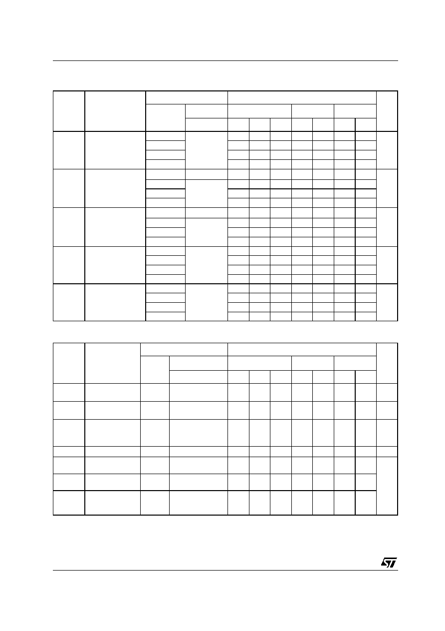
Table 6: AC Electrical Characteristics (C
L
= 35pF, R
L
= 50
,
t
r
= t
f
5ns)
Table 7: Analog Switch Characteristics (C
L
= 5pF, R
L
= 50
, T
A
= 25°C)
Note 1: Off Isolation = 20Log
10
(V
D
/V
S
), V
D
= output. V
S
= input to off switch
Symbol
Parameter
Test Condition
Value
Unit
V
CC
(V)
T
A
= 25°C
-40 to 85°C
-55 to 125°C
Min.
Typ.
Max.
Min.
Max.
Min.
Max.
t
PLH,
t
PHL
Propagation Delay
1.65-1.95
V
I
=OPEN
0.45
ns
2.3-2.7
0.40
3.0-3.6
0.30
3.6-4.3
0.30
t
ON
TURN-ON time
1.65-1.95
V
S
=0.8V
70
ns
2.3-2.7
V
S
=1.5V
30
50
60
3.0-3.6
30
50
60
3.6-4.3
30
50
60
t
OFF
TURN-OFF time
1.65-1.95
V
S
=0.8V
45
ns
2.3-2.7
V
S
=1.5V
25
30
40
3.0-3.6
25
30
40
3.6-4.3
25
30
40
t
D
Break Before Make
Time Delay
1.65-1.95
C
L
=35pF
R
L
= 50
V
S
=1.5V
ns
2.3-2.7
2
15
3.0-3.6
2
15
3.6-4.3
2
15
Q
Charge injection
1.65-1.95
C
L
= 100pF
R
L
= 1M
V
GEN
= 0V
R
GEN
= 0
pC
2.3-2.7
200
3.0-3.6
200
3.6-4.3
200
Symbol
Parameter
Test Condition
Value
Unit
V
CC
(V)
T
A
= 25°C
-40 to 85°C
-55 to 125°C
Min.
Typ.
Max.
Min.
Max.
Min.
Max.
OIRR
Off Isolation (1)
1.65-4.3
V
S
= 1V
RMS
f= 100KHz
-64
dB
Xtalk
Crosstalk
1.65-4.3
V
S
= 1V
RMS
f= 100KHz
-54
dB
THD
Total Harmonic
Distortion
2.3-4.3
R
L
= 600
V
IN
= 2V
PP
f= 20Hz to 20kHz
0.03
%
BW
-3dB Bandwidth
1.65-4.3
R
L
= 50
50
MHz
C
IN
Control Pin Input
Capacitance
5
pF
C
Sn
Sn Port Capaci-
tance
3.3
f= 1MHz
37
C
D
D Port Capaci-
tance when
Switch is Enabled
3.3
f= 1MHz
84
STG3699
5/12
Figure 2: On Resistance
Figure 3: Off Leakage
Figure 4: Off Isolation
Figure 5: Bandwidth
Figure 6: Channel To Channel Crosstalk
Document Outline