
PRELIMINARY DATA
This is preliminary information on a new product now in development or undergoing evaluation. Details are subject to
change without notice.
May 2006
Rev1
1/12
12
N-channel very fast PowerMESHTM IGBT
Lower on-voltage drop (V
cesat
)
Lower C
RES
/ C
IES
ratio (no cross-conduction
susceptbility)
Very soft ultra fast recovery antiparallel diode
High frequency operation up to 70 KHz
New generation products with tighter
parameter distribution
Compact design
Semitop
Æ
2 is a trademark of semikron
Description
Using the latest high voltage technology based on
a patented strip layout, STMicroelectronics has
designed an advanced family of IGBTs, the
PowerMESHTM IGBT, with outstanding
performances.
Applications
High frequency motor controls
Motor drivers
Internal schematic diagram
General features
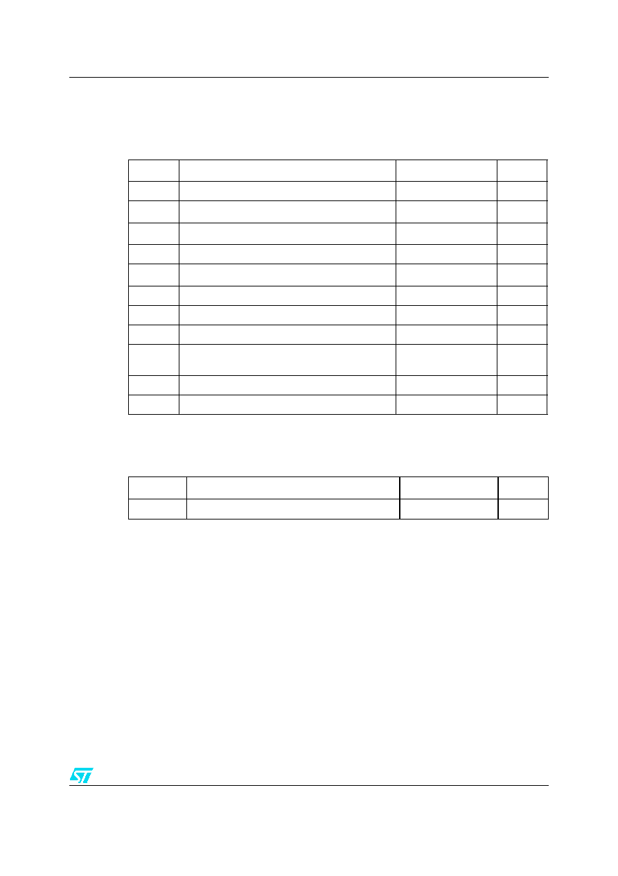
Type
V
CES
V
CE(sat)
(Max)
@ I
C
=7A,
Ts=25∞C
I
C
@80∞C
STG3P2M10N60B
600V
< 2.5V
10A
SEMITOPÆ2
STG3P2M10N60B
1-Phase bridge rectifier + 3 phase inverter
IGBT - SEMITOP
Æ
2 module
www.st.com
Order codes
Sales type
Marking
Package
Packaging
STG3P2M10N60B
G3P2M10N60B
SEMITOPÆ2
SEMIBOX

Contents
STG3P2M10N60B
2/12
Contents
1
Electrical ratings . . . . . . . . . . . . . . . . . . . . . . . . . . . . . . . . . . . . . . . . . . . . 3
2
Electrical characteristics . . . . . . . . . . . . . . . . . . . . . . . . . . . . . . . . . . . . . 4
2.1
Typical characteristics (curves) . . . . . . . . . . . . . . . . . . . . . . . . . . . . . . . . . 7
3
Test circuit . . . . . . . . . . . . . . . . . . . . . . . . . . . . . . . . . . . . . . . . . . . . . . . . 8
4
Package mechanical data . . . . . . . . . . . . . . . . . . . . . . . . . . . . . . . . . . . . . 9
5
Revision history . . . . . . . . . . . . . . . . . . . . . . . . . . . . . . . . . . . . . . . . . . . 11
STG3P2M10N60B
Electrical ratings
3/12
1 Electrical
ratings
Table 1.
Absolute maximum ratings
Symbol
Parameter
Value
Unit
V
CES
Collector-emitter voltage (V
GS
= 0)
600
V
I
C
(1)
1.
Calculated value
Collector current (continuous) at Ts = 25∞C
19
A
I
C
(1)
Collector current (continuous) at Ts = 80∞C
10
A
V
GE
Gate-emitter Voltage
±20
V
I
CM
(2)
2.
Pulse width limited by max. junction temperature
T
P
<1ms; T
s
=25∞C
38
A
I
CM
T
P
<1ms; T
s
=80∞C
20
A
I
F
Diode RMS forward current at Ts = 25∞C
19
A
P
TOT
Total dissipation at Ts = 25∞C
56
W
V
ISO
Insulation withstand voltage A.C.
(t=1min/sec; Ts=25∞C)
2500/3000
V
T
stg
Storage temperature
≠ 40 to 125
∞C
T
j
Operating junction temperature
≠ 40 to 150
∞C
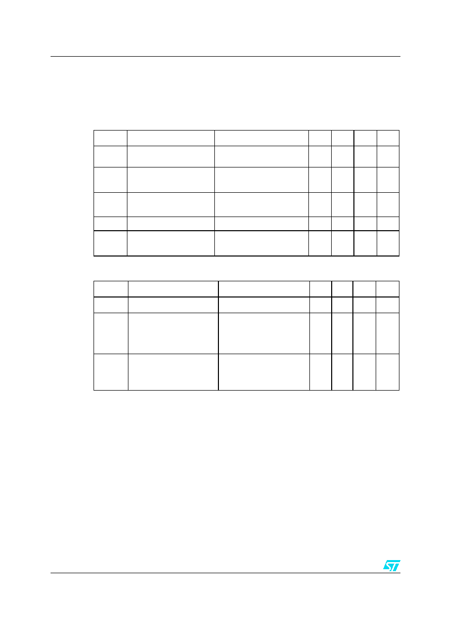
Table 2.
Thermal resistance
Symbol
Parameter
Value
Unit
Rth(j-s)
Thermal resistance junction-sink
(1)
Max.
1.
Resistance value with conductive grease applied and maximum mounting torque equal to 2Nm
2.2
K/W
Electrical characteristics
STG3P2M10N60B
4/12
2 Electrical
characteristics
(T
S
=25∞C unless otherwise specified)
Table 3.
Static
Symbol
Parameter
Test condictions
Min.
Typ.
Max.
Unit
V
BR(CES)
Collector-emitter
breakdown voltage
I
C
= 1mA, V
GE
= 0
600
V
I
CES
Collector cut-off current
(V
GE
= 0)
V
CE
= Max rating,T
S
= 25∞C
V
CE
=Max rating,T
S
= 125∞C
10
1
µA
mA
I
GES
Gate-Emitter Leakage
Current (V
CE
= 0)
V
GE
= ±20V , V
CE
= 0
±100
nA
V
GE(th)
Gate Threshold Voltage
V
CE
= V
GE
, I
C
= 250µA
3.75
5.75
V
V
CE(sat)
Collector-emitter saturation
voltage
V
GE
= 15V, I
C
= 7A
V
GE
= 15V, I
C
= 7A, Tc= 125∞C
1.85
1.7
2.5
V
V
Table 4.
Dynamic
Symbol
Parameter
Test condictions
Min.
Typ.
Max.
Unit
g
fs
(1)
1.
Pulsed: pulse duration=300µs, duty cycle 1.5%
Forward transconductance
V
CE
= 15V
,
I
C
= 7A
4.30
S
C
ies
C
oes
C
res
Input capacitance
Output capacitance
Reverse transfer
capacitance
V
CE
= 25V, f = 1MHz,
V
GE
= 0
720
81
17
pF
pF
pF
Q
g
Q
ge
Q
gc
Total gate charge
Gate-emitter charge
Gate-collector charge
V
CE
= 390V, I
C
= 5A,
V
GE
= 15V,
(see Figure 8)
35
7
16
48
nC
nC
nC

STG3P2M10N60B
Electrical characteristics
5/12
Table 5.
Switching on/off
Symbol
Parameter
Test condictions
Min.
Typ.
Max.
Unit
t
d(on)
t
r
(di/dt)
on
Turn-on delay time
Current rise time
Turn-on current slope
V
CC
= 300V, I
C
= 7A
R
G
= 22
, V
GE
= ±15V
T
S
= 25∞C
(see Figure 9)
18.5
8.5
1060
ns
ns
A/µs
t
d(on)
t
r
(di/dt)
on
Turn-on delay time
Current rise time
Turn-on current slope
V
CC
= 300V, I
C
= 7A
R
G
= 22
, V
GE
= ±15V
T
S
=125∞C
(see Figure 9)
18.5
7
1000
ns
ns
A/µs
t
r
(V
off
)
t
d
(
off
)
t
f
Off voltage rise time
Turn-off delay time
Current fall time
V
CC
= 300V, I
C
= 7A
R
G
= 22
, V
GE
= ±15V
T
S
=25∞C
(see Figure 9)
27
72
60
ns
ns
ns
t
r
(V
off
)
t
d
(
off
)
t
f
Off voltage rise time
Turn-off delay time
Current fall time
V
CC
= 300V, I
C
= 7A
R
G
= 22
, V
GE
= ±15V
T
S
=125∞C
(see Figure 9)
56
116
105
ns
ns
ns
Table 6.
Switching energy (inductive load)
Symbol
Parameter
Test condictions
Min.
Typ.
Max.
Unit
E
on
(1)
E
off
(2)
E
ts
1.
Eon is the tun-on losses when a typical diode is used in the test circuit in figure 2. If the IGBT is offered in
a package with a co-pak diode, the co-pack diode is used as external diode. IGBTs & Diode are at the
same temperature (25∞C and 125∞C)
2.
Turn-off losses include also the tail of the collector current
Turn-on switching losses
Turn-off switching losses
Total switching losses
V
CC
= 300V, I
C
= 7A
R
G
= 22
, V
GE
= ±15V
T
S
=25∞C
(see Figure 9)
95
115
210
µJ
µJ
µJ
E
on
(1)
E
off
(2)
E
ts
Turn-on switching losses
Turn-off switching losses
Total switching losses
V
CC
= 300V, I
C
= 7A
R
G
= 22
, V
GE
= ±15V
T
S
= 125∞C
(see Figure 9)
140
215
355
µJ
µJ
µJ