STGB10N60L
N-CHANNEL 10A - 600V D
2
PAK
LOGIC LEVEL IGBT
s
HIGH INPUT IMPEDANCE
(VOLTAGE DRIVEN)
s
VERY LOW ON-VOLTAGE DROP (V
cesat
)
s
LOW THRESHOLD VOLTAGE
(LOGIC LEVEL INPUT)
s
HIGH CURRENT CAPABILITY
s
OFF LOSSES INCLUDE TAIL CURRENT
s
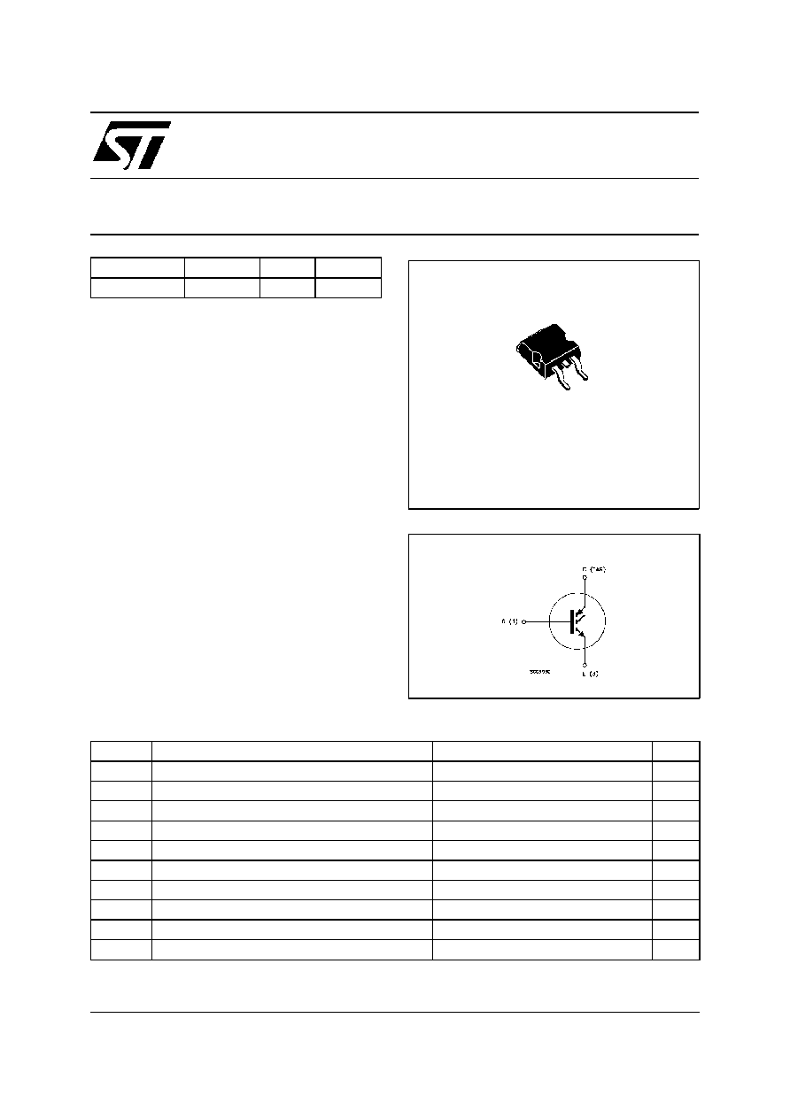
SURFACE-MOUNTING D2PAK (TO-263)
POWER PACKAGE IN TUBE (NO SUFFIX)
OR IN TAPE & REEL (SUFFIX "T4")
APPLICATIONS
s
ELECTRONIC IGNITION
s
LIGHT DIMMER
s
STATIC RELAYS
Æ
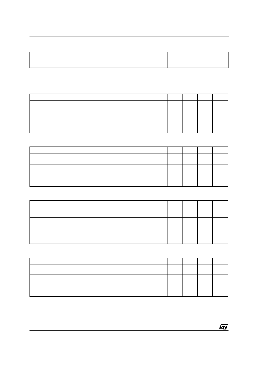
INTERNAL SCHEMATIC DIAGRAM
ABSOLUTE MAXIMUM RATINGS
Symb ol
Parameter
Value
Un it
V
CES
Collector-Emitter Volt age (V
G S
= 0)
600
V
V
ECR
Reverse Batt ery Prot ection
25
V
V
GE
G ate-Emitter Voltage
±
15
V
I
C
Collector Current (continuous) at T
c
= 25
o
C
25
A
I
C
Collector Current (continuous) at T
c
= 100
o
C
20
A
I
CM
(
∑
)
Collector Current (pulsed)
100
A
P
tot
T otal Dissipation at T
c
= 25
o
C
125
W
Derating Fact or
0. 83
W /
o
C
T
s tg
Storage T emperature
-65 t o 175
o
C
T
j
Max. Operating Junction Temperat ure
175
o
C
(
∑
) Pulse width limited by safe operating area
TYPE
V
CES
V
CE(sat )
I
C
STGB10N60L
600 V
< 1.95 V
10 A
June 1999
1
3
D
2
PAK
TO-263
1/8
THERMAL DATA
R
thj -case
R
thj -amb
R
thc-sink
Thermal Resistance Junction-case
Max
Thermal Resistance Junction-ambient
Max
Thermal Resistance Case-sink
T yp
1.2
62. 5
0.1
o
C/W
o
C/W
o
C/W
ELECTRICAL CHARACTERISTICS (T
j
= - 40 to 150
o
C unless otherwise specified)
OFF
Symbo l
Parameter
Test Con ditions
Min.
Typ.
Max.
Unit
V
BR(c es)
Collector-Emitt er
Breakdown Voltage
I
C
= 250
µ
A
V
GE
= 0
600
V
I
CES
Collector cut-of f
(V
G E
= 0)
V
CE
= Max Rat ing
T
j
=
25
o
C
V
CE
= Max Rat ing
T
j
= 125
o
C
25
100
µ
A
µ
A
I
G ES
Gat e-Emitter Leakage
Current (V
CE
= 0)
V
GE
=
±
15 V
V
CE
= 0
±
100
nA
ON (
)
Symbo l
Parameter
Test Con ditions
Min.
Typ.
Max.
Unit
V
G E(th)
Gat e Threshold
Voltage
V
CE
= V
GE
I
C
= 250
µ
A
V
CE
= V
GE
I
C
= 250
µ
A T
j
= 25
o
C
0. 6
1. 0
2. 4
2. 0
V
V
V
CE(SAT )
Collector-Emitt er
Sat uration Voltage
V
GE
= 4. 5 V
I
C
= 8 A
T
j
= - 40
o
C
V
GE
= 4. 5 V
I
C
= 9.5 A T
j
=
25
o
C
V
GE
= 4. 5 V
I
C
= 8 A
T
j
= 150
o
C
1.5
1.4
1.25
2. 0
V
V
V
I
C
Collector Current
V
GE
= 4. 5 V
V
CE
= 7 V
15
45
A
DYNAMIC
Symbo l
Parameter
Test Con ditions
Min.
Typ.
Max.
Unit
g
f s
Forward
Transconductance
V
CE
=25 V
I
C
= 8 A
T
j
=
25
o
C
7
12
S
C
i es
C
o es
C
res
Input Capacitance
Out put Capacitance
Reverse Transfer
Capacitance
V
CE
= 25 V
f = 1 MHz
V
GE
= 0
1800
120
19
2600
165
26
pF
pF
pF
Q
G
Gat e Charge
V
CE
= 400 V
I
C
= 8 A
V
GE
= 5 V
30
nC
FUNCTIONAL CHARACTERISTICS
Symbo l
Parameter
Test Con ditions
Min.
Typ.
Max.
Unit
I
CL
Lat ching Current
V
clamp
= 480 V
dV/ dt = 200 V/
µ
s
T
j
= 125
o
C
20
A
E
CF
Forward Clamping
Energy
T
start
= 55
o
C
V
cl amp
= 480 V
I
C
= 10 A
L = 4.2 mH - Single Pulse
210
mJ
E
AR
Reverse Avalanche
Energy
10
mJ
STGB10N60L
2/8
ELECTRICAL CHARACTERISTICS (continued)
SWITCHING ON
Symbo l
Parameter
Test Con ditions
Min.
Typ.
Max.
Unit
t
d(on)
t
r
Delay Time
Rise Time
V
CC
= 480 V
I
C
= 8 A
V
GE
= 5 V
R
G
= 1 K
0.7
1.9
µ
s
µ
s
(di/dt)
on
E
o n
Turn-on Current Slope
Turn-on
Switching Losses
V
CC
= 480 V
I
C
= 8 A
R
G
= 1 K
V
GE
= 5 V
T
j
= 125
o
C
5
2.5
A/
µ
s
mJ
SWITCHING OFF
Symbo l
Parameter
Test Con ditions
Min.
Typ.
Max.
Unit
t
c
t
r
(v
off
)
t
f
E
o ff
(**)
Cross-O ver Time
Off Volt age Rise Time
Fall T ime
Turn-off Swit ching Loss
V
CC
= 480 V
I
C
= 8 A
R
G E
= 1 K
V
G E
= 5 V
T
j
= 25
o
C
4
2.5
1.5
9.0
µ
s
µ
s
µ
s
mJ
t
c
t
r
(v
off
)
t
f
E
o ff
(**)
Cross-O ver Time
Off Volt age Rise Time
Fall T ime
Turn-off Swit ching Loss
V
CC
= 480 V
I
C
= 8 A
R
G E
= 1 K
V
G E
= 5 V
T
j
= 125
o
C
6
3.3
2.5
10.8
µ
s
µ
s
µ
s
mJ
(
∑
) Pulse width limited by safe operating area
(
) Pulsed: Pulse duration = 300
µ
s, duty cycle 1.5 %
(**)Losses Include Also The Tail (Jedec Standardization)
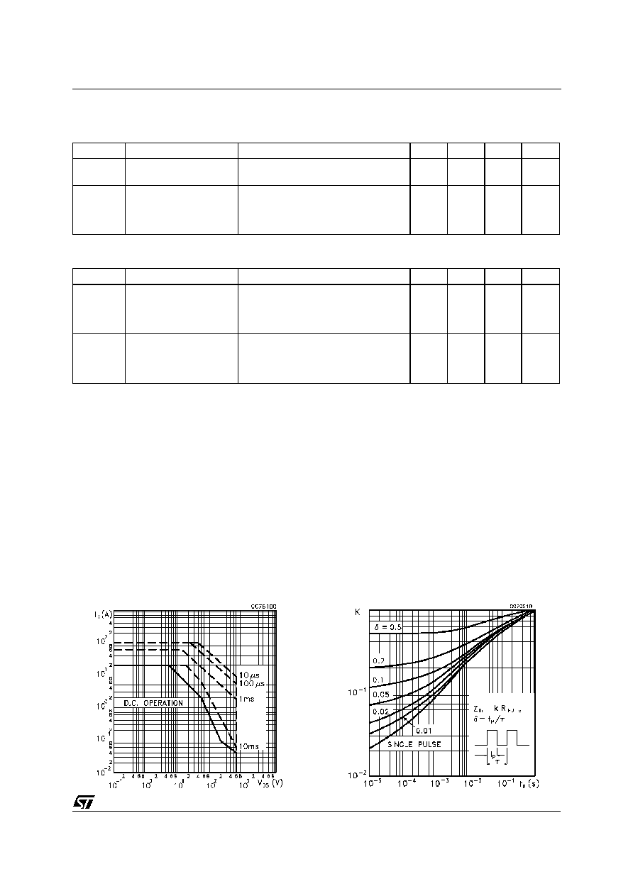
Safe Operating Area
Thermal Impedance
STGB10N60L
3/8
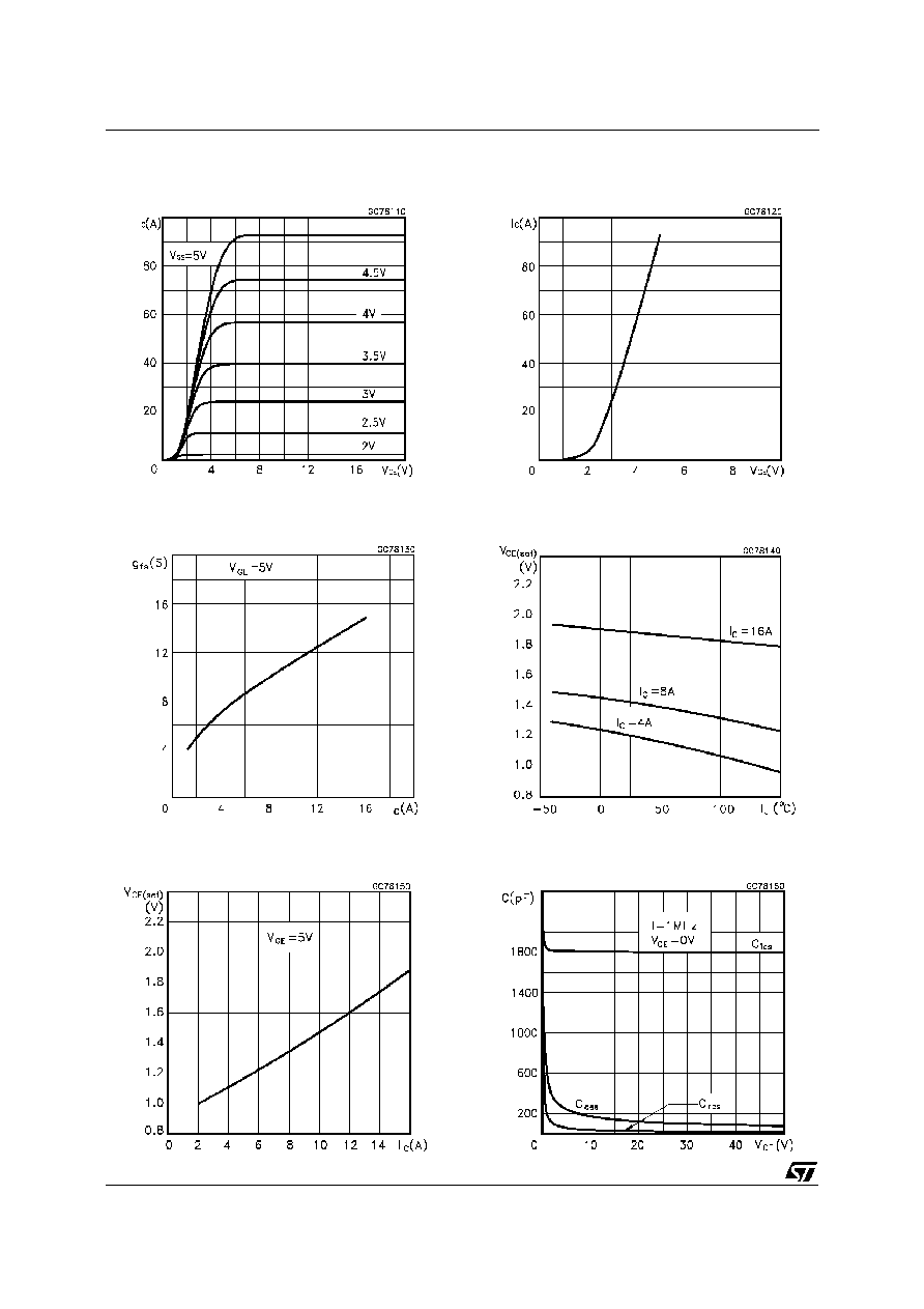
Output Characteristics
Transconductance
Collector-Emitter On Voltage vs Collector
Current
Transfer Characteristics
Collector-Emitter On Voltage vs Temperature
Capacitance Variations
STGB10N60L
4/8
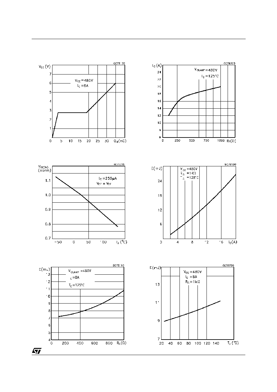
Gate Charge vs Gate-Emitter Voltage
Gate Threshold vs Temperature
Off Losses vs Gate Resistance
Latching Current vs Rg
Off Losses vs Collector Current
Off Losses vs Temperature
STGB10N60L
5/8

Switching Off Safe Operatin Area
Fig. 1: Gate Charge test Circuit
Fig. 2: Switching Times Test Circuit For
Resistive Load
Fig. 3: Test Circuit For Inductive Load Switching
STGB10N60L
6/8

DIM.
mm
inch
MIN.
TYP.
MAX.
MIN.
TYP.
MAX.
A
4.4
4.6
0.173
0.181
A1
2.49
2.69
0.098
0.106
B
0.7
0.93
0.027
0.036
B2
1.14
1.7
0.044
0.067
C
0.45
0.6
0.017
0.023
C2
1.21
1.36
0.047
0.053
D
8.95
9.35
0.352
0.368
E
10
10.4
0.393
0.409
G
4.88
5.28
0.192
0.208
L
15
15.85
0.590
0.624
L2
1.27
1.4
0.050
0.055
L3
1.4
1.75
0.055
0.068
L2
L3
L
B2
B
G
E
A
C2
D
C
A1
DETAIL "A"
DETAIL "A"
A2
P011P6/E
TO-263 (D
2
PAK) MECHANICAL DATA
STGB10N60L
7/8

Information furnished is believ ed to be accurate and reliable. However, STMicroelectronics assumes no responsibil ity for the consequences
of use of such information nor for any infringement of patents or other rights of third parties which may result from its use. No license is
granted by implication or otherwise under any patent or patent rights of STMicroelectronics. Specific ation mentioned in this publication are
subjec t to change without notice. This publication supersedes and replaces all information previously supplied. STMicroelectronics products
are not authorized for use as critical components in life support devices or systems without express written approval of STMicroelectronics.
The ST logo is a trademark of STMicroelectronics
©
1999 STMicroelectronics ≠ Printed in Italy ≠ All Rights Reserved
STMicroelectronics GROUP OF COMPANIES
Australia - Brazil - China - Finland - France - Germany - Hong Kong - India - Italy - Japan - Malaysia - Malta - Morocco -
Singapore - Spain - Sweden - Switzerland - United Kingdom - U.S.A.
http://www.st.com
.
STGB10N60L
8/8