1/11
December 2002
STGB20NB32LZ
STGB20NB32LZ-1
N-CHANNEL CLAMPED 20A - D
2
PAK/I
2
PAK
INTERNALLY CLAMPED PowerMESHTM IGBT
s
POLYSILICON GATE VOLTAGE DRIVEN
s
LOW THRESHOLD VOLTAGE
s
LOW ON-VOLTAGE DROP
s
HIGH CURRENT CAPABILITY
s
HIGH VOLTAGE CLAMPING FEATURE
s
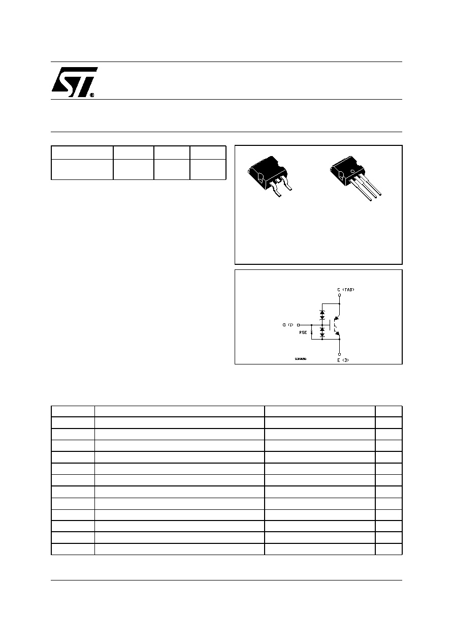
SURFACE-MOUNTING D≤PAK (TO-263)
POWER PACKAGE IN TUBE (NO SUFFIX) OR
IN TAPE & REEL (SUFFIX "T4")
DESCRIPTION
Using the latest high voltage technology based on a
patented strip layout, STMicroelectronics has
designed an advanced family of IGBTs, the
PowerMESH
TM
IGBTs, with outstanding
performances. The built in collector-gate zener
exhibits a very precise active clamping while the
gate-emitter zener supplies an ESD protection.
APPLICATIONS
s
AUTOMOTIVE IGNITION
ABSOLUTE MAXIMUM RATINGS
(∑)Pulse width limited by safe operating area
TYPE
V
CES
V
CE(sat)
I
C
STGB20NB32LZ
STGB20NB32LZ-1
CLAMPED
CLAMPED
< 2.0
V
< 2.0
V
20 A
20 A
Symbol
Parameter
Value
Unit
V
CES
Collector-Emitter Voltage (V
GS
= 0)
CLAMPED
V
V
ECR
Reverse Battery Protection
20
V
V
GE
Gate-Emitter Voltage
CLAMPED
V
I
C
Collector Current (continuous) at T
c
= 25∞C
40
A
I
C
Collector Current (continuous) at T
c
= 100∞C
30
A
I
CM
( )
Collector Current (pulsed)
80
A
Eas
Single Pulse Energy T
c
= 25∞C
700
mJ
P
tot
Total Dissipation at T
c
= 25∞C
150
W
Derating Factor
1
W/∞C
E
SD
ESD (Human Body Model)
4
KV
T
stg
Storage Temperature
≠65 to 175
∞C
T
j
Max. Operating Junction Temperature
175
∞C
1
3
D
2
PAK
1
2
3
I
2
PAK
INTERNAL SCHEMATIC DIAGRAM
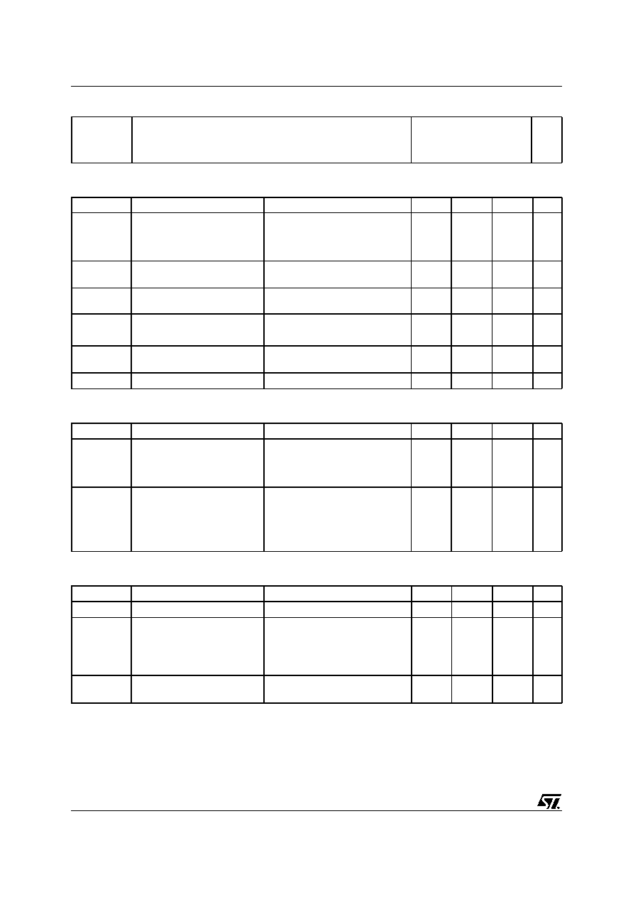
STGB20NB32LZ - STGB20NB32LZ-1
2/11
THERMAL DATA
ELECTRICAL CHARACTERISTICS (T
CASE
= 25 ∞C UNLESS OTHERWISE SPECIFIED)
OFF
ON (1)
DYNAMIC
Rthj-case
Thermal Resistance Junction-case Max
1
∞C/W
Rthj-amb
Thermal Resistance Junction-ambient Max
62.5
∞C/W
Rthc-sink
Thermal Resistance Case-sink Typ
0.2
∞C/W
Symbol
Parameter
Test Conditions
Min.
Typ.
Max.
Unit
BV
(CES)
Clamped Voltage
I
C
= 2 mA, V
GE
= 0, Tc= - 40∞C
330
355
380
V
I
C
= 2 mA, V
GE
= 0, Tc= 25∞C
325
350
375
V
I
C
= 2 mA, V
GE
= 0, Tc= 150∞C
320
345
370
V
BV
(ECR)
Emitter Collector Break-down
Voltage
I
C
= 75 mA, Tc = 25∞C
20
28
V
BV
GE
Gate Emitter Break-down
Voltage
I
G
= ± 2 mA
12
14
16
V
I
CES
Collector cut-off Current
(V
GE
= 0)
V
CE
= 15 V, V
GE
=0 ,T
C
=150 ∞C
10
µA
V
CE
=200 V, V
GE
=0 ,T
C
=150∞C
100
µA
I
GES
Gate-Emitter Leakage
Current (V
CE
= 0)
V
GE
= ± 10V , V
CE
= 0
± 400
± 660
± 1000
µA
R
GE
Gate Emitter Resistance
10
15
25
K
Symbol
Parameter
Test Conditions
Min.
Typ.
Max.
Unit
V
GE(th)
Gate Threshold Voltage
V
CE
= V
GE
, I
C
= 250µA, Tc=-40∞C
1.2
1.4
2
V
V
CE
= V
GE
, I
C
= 250µA, Tc= 25∞C
1
V
V
CE
=V
GE
, I
C
= 250µA, Tc=150∞C
0.6
V
V
CE(SAT)
Collector-Emitter Saturation
Voltage
V
GE
=4.5V, I
C
= 10 A, Tc= 25∞C
1.1
1.8
V
V
GE
=4.5V, I
C
= 10 A, Tc= 150∞C
1
1.7
V
V
GE
=4.5V, I
C
= 20 A, Tc= 25∞C
1.35
2
V
V
GE
=4.5V, I
C
= 20 A, Tc= 150∞C
1.25
2
V
Symbol
Parameter
Test Conditions
Min.
Typ.
Max.
Unit
g
fs
Forward Transconductance
V
CE
= 25 V
,
I
C
=20 A
35
S
C
ies
Input Capacitance
V
CE
= 25 V, f = 1 MHz, V
GE
= 0
2300
pF
C
oes
Output Capacitance
165
pF
C
res
Reverse Transfer
Capacitance
28
pF
Q
g
Gate Charge
V
CE
= 280 V, I
C
= 20 A,
V
GE
= 5 V
51
nC
3/11
STGB20NB32LZ - STGB20NB32LZ-1
FUNCTIONAL CHARACTERISTICS
SWITCHING ON
SWITCHING OFF
(**)Losses Include Also the Tail (jedec Standardization)
Symbol
Parameter
Test Conditions
Min.
Typ.
Max.
Unit
II
Latching Current
V
Clamp
= 250 V, T
C
= 150 ∞C
R
GOFF
= 1K
, V
GE
= 4.5 V
80
A
U.I.S.
Functional Test Open
Secondary Coil
R
GOFF
= 1K
, L = 3 mH ,Tc=25∞C
R
GOFF
=1K
, L = 3mH ,Tc=150∞C
21.6
15
26
18
A
A
Symbol
Parameter
Test Conditions
Min.
Typ.
Max.
Unit
t
d(on)
t
r
Delay Time
Rise Time
V
CC
= 250 V, I
C
= 20 A
R
G
= 1K
, V
GE
= 4.5 V
2.3
0.6
µs
µs
(di/dt)
on
Turn-on Current Slope
V
CC
= 250 V, I
C
= 20 A
R
G
=1K
, V
GE
= 4.5 V
550
A/µs
Eon
Turn-on Switching Losses
V
CC
= 250 V, I
C
= 20 A, Tc=25∞C
R
G
=1K
, V
GE
= 4.5 V, Tc=150∞C
8.8
9.2
mJ
mJ
Symbol
Parameter
Test Conditions
Min.
Typ.
Max.
Unit
t
c
Cross-Over Time
V
cc
= 250 V, I
C
= 20 A,
R
GE
= 1 K
, V
GE
= 4.5 V
4.8
µs
t
r
(V
off
)
Off Voltage Rise Time
2.6
µs
t
f
Fall Time
2
µs
t
d
(
off
)
Off Voltage Delay Time
11.5
µs
E
off
(**)
Turn-off Switching Loss
11.8
mJ
t
c
Cross-Over Time
V
cc
= 250 V, I
C
= 20 A,
R
GE
= 1 K
, V
GE
= 4.5 V
Tc = 150 ∞C
7.8
µs
t
r
(V
off
)
Off Voltage Rise Time
3.5
µs
t
f
Fall Time
3.9
µs
t
d
(
off
)
Off Voltage Delay Time
12
µs
E
off
(**)
Turn-off Switching Loss
17.8
mJ
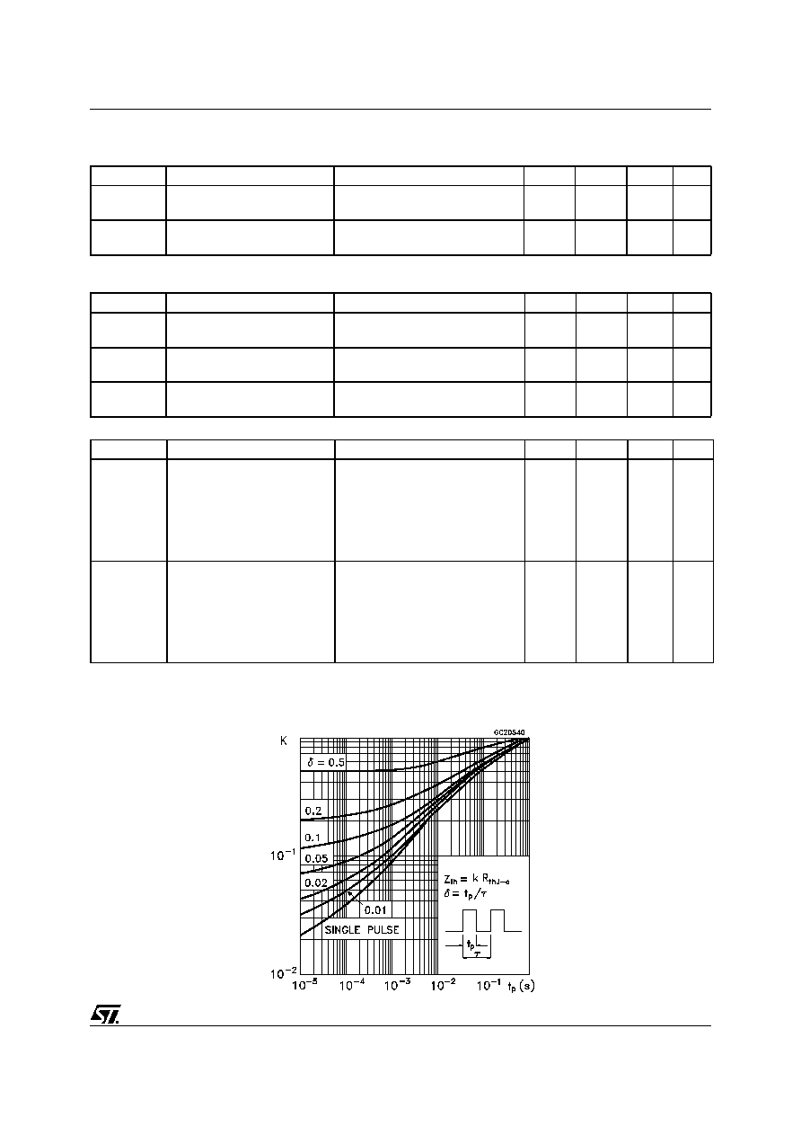
Thermal Impedance
STGB20NB32LZ - STGB20NB32LZ-1
4/11
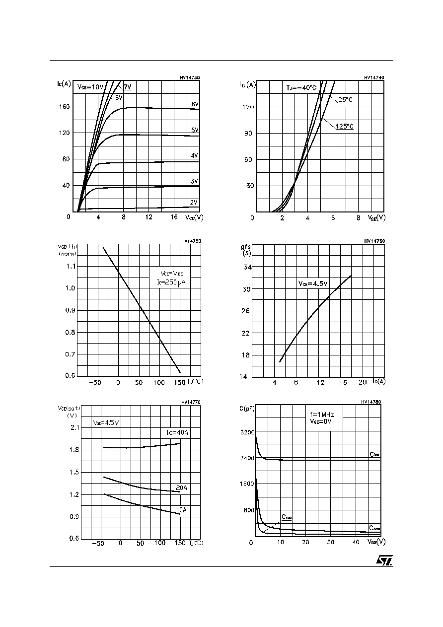
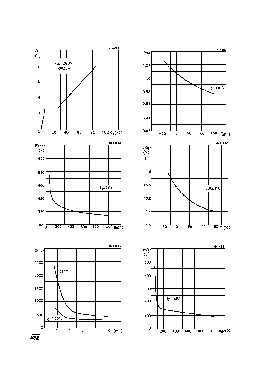
Output Characteristics
Transconductance
Normalized Gate Threshold Voltage vs Temp.
Transfer Characteristics
Collector-Emitter On Voltage vs Temperature
Capacitance Variations
5/11
STGB20NB32LZ - STGB20NB32LZ-1
dV/dt Gate-Emitter Resistance
B
VGEO
(Zener Gate-Emitter) vs Temperature
Gate Charge vs Gate-Emitter Voltage
Break-Down Voltage vs Emitter Resistance
Normalized BreakDown Voltage vs Temperature
Self Clamped Inductive Switching Energy vs
Open Secondary Coil
STGB20NB32LZ - STGB20NB32LZ-1
6/11
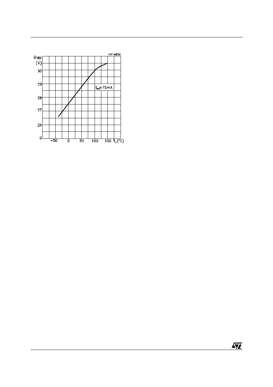
B
VEC
Reverse Battery Voltage
7/11
STGB20NB32LZ - STGB20NB32LZ-1
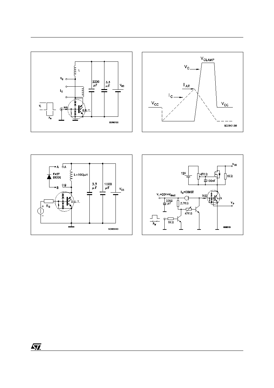
Fig. 4: Gate Charge test Circuit
Fig. 3: Test Circuit For Inductive Load Switching
And Diode Recovery Times
Fig. 2: Unclamped Inductive Waveform
Fig. 1: Unclamped Inductive Load Test Circuit
STGB20NB32LZ - STGB20NB32LZ-1
8/11
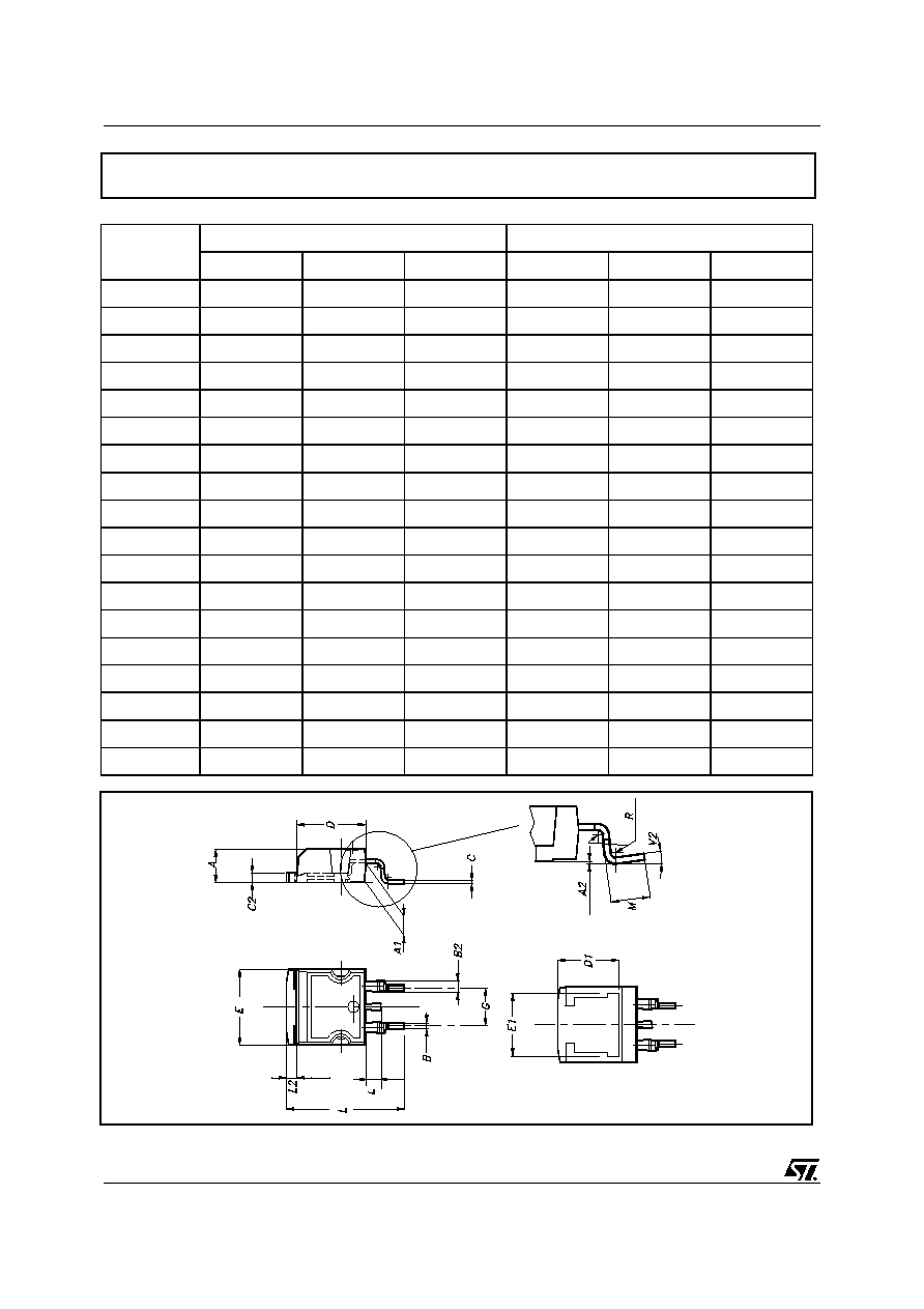
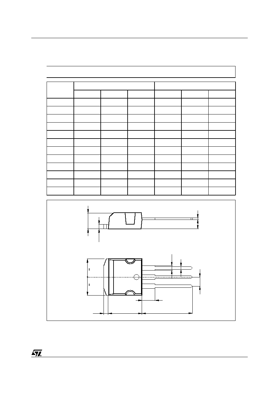
1
DIM.
mm.
inch
MIN.
TYP
MAX.
MIN.
TYP.
MAX.
A
4.4
4.6
0.173
0.181
A1
2.49
2.69
0.098
0.106
A2
0.03
0.23
0.001
0.009
B
0.7
0.93
0.027
0.036
B2
1.14
1.7
0.044
0.067
C
0.45
0.6
0.017
0.023
C2
1.23
1.36
0.048
0.053
D
8.95
9.35
0.352
0.368
D1
8
0.315
E
10
10.4
0.393
E1
8.5
0.334
G
4.88
5.28
0.192
0.208
L
15
15.85
0.590
0.625
L2
1.27
1.4
0.050
0.055
L3
1.4
1.75
0.055
0.068
M
2.4
3.2
0.094
0.126
R
0.4
0.015
V2
0∫
8∫
D
2
PAK MECHANICAL DATA
3
9/11
STGB20NB32LZ - STGB20NB32LZ-1
DIM.
mm
inch
MIN.
TYP.
MAX.
MIN.
TYP.
MAX.
A
4.4
4.6
0.173
0.181
A1
2.49
2.69
0.098
0.106
B
0.7
0.93
0.027
0.036
B2
1.14
1.7
0.044
0.067
C
0.45
0.6
0.017
0.023
C2
1.23
1.36
0.048
0.053
D
8.95
9.35
0.352
0.368
e
2.4
2.7
0.094
0.106
E
10
10.4
0.393
0.409
L
13.1
13.6
0.515
0.531
L1
3.48
3.78
0.137
0.149
L2
1.27
1.4
0.050
0.055
L
L1
B2
B
D
E
A
C2
C
A1
L2
e
P011P5/E
TO-262 (I
2
PAK) MECHANICAL DATA

STGB20NB32LZ - STGB20NB32LZ-1
10/11
TAPE AND REEL SHIPMENT (suffix "T4")*
TUBE SHIPMENT (no suffix)*
D
2
PAK FOOTPRINT
* on sales type
DIM.
mm
inch
MIN.
MAX.
MIN.
MAX.
A
330
12.992
B
1.5
0.059
C
12.8
13.2
0.504
0.520
D
20.2
0795
G
24.4
26.4
0.960
1.039
N
100
3.937
T
30.4
1.197
BASE QTY
BULK QTY
1000
1000
REEL MECHANICAL DATA
DIM.
mm
inch
MIN.
MAX.
MIN.
MAX.
A0
10.5
10.7
0.413
0.421
B0
15.7
15.9
0.618
0.626
D
1.5
1.6
0.059
0.063
D1
1.59
1.61
0.062
0.063
E
1.65
1.85
0.065
0.073
F
11.4
11.6
0.449
0.456
K0
4.8
5.0
0.189
0.197
P0
3.9
4.1
0.153
0.161
P1
11.9
12.1
0.468
0.476
P2
1.9
2.1
0.075
0.082
R
50
1.574
T
0.25
0.35
0.0098 0.0137
W
23.7
24.3
0.933
0.956
TAPE MECHANICAL DATA

11/11
STGB20NB32LZ - STGB20NB32LZ-1
Information furnished is believed to be accurate and reliable. However, STMicroelectronics assumes no responsibility for the
consequences of use of such information nor for any infringement of patents or other rights of third parties which may result from
its use. No license is granted by implication or otherwise under any patent or patent rights of STMicroelectronics. Specifications
mentioned in this publication are subject to change without notice. This publication supersedes and replaces all information
previously supplied. STMicroelectronics products are not authorized for use as critical components in life support devices or
systems without express written approval of STMicroelectronics.
© The ST logo is a registered trademark of STMicroelectronics
© 2002 STMicroelectronics - Printed in Italy - All Rights Reserved
STMicroelectronics GROUP OF COMPANIES
Australia - Brazil - Canada - China - Finland - France - Germany - Hong Kong - India - Israel - Italy - Japan - Malaysia - Malta - Morocco
Singapore - Spain - Sweden - Switzerland - United Kingdom - United States.
© http://www.st.com