1/11
June 2003
STGP3NB60MD - STGB3NB60MD
N-CHANNEL 3A - 600V
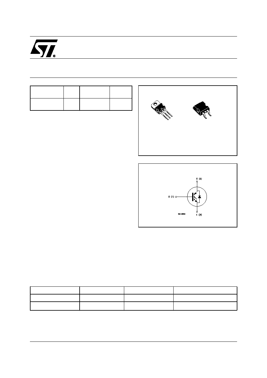
TO-220 / D
2
PAK
PowerMESHTM IGBT
s
HIGH INPUT IMPEDANCE
s
LOW ON-VOLTAGE DROP (V
cesat
)
s
OFF LOSSES INCLUDE TAIL CURRENT
s
LOW GATE CHARGE
s
HIGH CURRENT CAPABILITY
s
HIGH FREQUENCY OPERATION
s
CO-PACKAGED WITH TURBOSWITCHTM
ANTIPARALLEL DIODE
DESCRIPTION
Using the latest high voltage technology based on a
patented strip layout, STMicroelectronics has de-
signed an advanced family of IGBTs, the Power-
MESHTM IGBTs, with outstanding perfomances.
The suffix "M" identifies a family optimized to
achieve very low switching switching times for high
frequency applications (<20KHZ)
APPLICATIONS
s
MOTOR CONTROLS
s
SMPS AND PFC AND BOTH HARD SWITCH
AND RESONANT TOPOLOGIES
ORDERING INFORMATION
TYPE
V
CES
V
CE(sat) (Max)
@25∞C
I
C
@100∞C
STGP3NB60MD
STGB3NB60MD
600 V
600 V
< 1.9
V
< 1.9V
3 A
3 A
SALES TYPE
MARKING
PACKAGE
PACKAGING
STGP3NB60MD
GP3NB60MD
TO-220
TUBE
STGB3NB60MDT4
GB3NB60MD
D
2
PAK
TAPE & REEL
TO-220
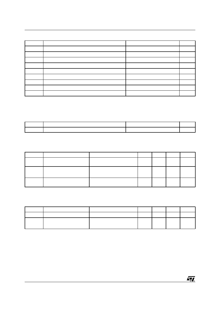
1
2
3
D
2
PAK
1
3
INTERNAL SCHEMATIC DIAGRAM
STGP3NB60MD - STGB3NB60MD
2/11
ABSOLUTE MAXIMUM RATINGS
( )
Pulse width limited by safe operating area
THERMAL DATA
ELECTRICAL CHARACTERISTICS (T
CASE
= 25 ∞C UNLESS OTHERWISE SPECIFIED)
OFF
ON (1)
Symbol
Parameter
Value
Unit
V
CES
Collector-Emitter Voltage (V
GS
= 0)
600
V
V
GE
Gate-Emitter Voltage
±20
V
I
C
Collector Current (continuous) at T
C
= 25∞C
6
A
I
C
Collector Current (continuous) at T
C
= 100∞C
3
A
I
CM
( )
Collector Current (pulsed)
24
A
P
TOT
Total Dissipation at T
C
= 25∞C
68
W
Derating Factor
0.55
W/∞C
T
stg
Storage Temperature
≠ 55 to 150
∞C
T
j
Max. Operating Junction Temperature
150
∞C
Rthj-case
Thermal Resistance Junction-case Max
1.8
∞C/W
Rthj-amb
Thermal Resistance Junction-ambient Max
62.5
∞C/W
Symbol
Parameter
Test Conditions
Min.
Typ.
Max.
Unit
V
BR(CES)
Collector-Emitter Breakdown
Voltage
I
C
= 250 µA, V
GE
= 0
600
V
I
CES
Collector cut-off
(V
GE
= 0)
V
CE
= Max Rating, T
C
= 25 ∞C
50
µA
V
CE
= Max Rating, T
C
= 125 ∞C
100
µA
I
GES
Gate-Emitter Leakage
Current (V
CE
= 0)
V
GE
= ± 20V , V
CE
= 0
±100
nA
Symbol
Parameter
Test Conditions
Min.
Typ.
Max.
Unit
V
GE(th)
Gate Threshold Voltage
V
CE
= V
GE
, I
C
= 250 µA
3
5
V
V
CE(sat)
Collector-Emitter Saturation
Voltage
V
GE
= 15V, I
C
= 3 A
1.5
1.9
V
V
GE
= 15V, I
C
= 3 A, Tj =125∞C
1.2
V
3/11
STGP3NB60MD - STGB3NB60MD
ELECTRICAL CHARACTERISTICS (CONTINUED)
DYNAMIC
SWITCHING ON
SWITCHING OFF
COLLECTOR-EMITTER DIODE
Note: 1. Pulsed: Pulse duration = 300 µs, duty cycle 1.5 %.
2. Pulse width limited by max. junction temperature.
(**)Losses include Also the Tail (Jedec Standardization)
Symbol
Parameter
Test Conditions
Min.
Typ.
Max.
Unit
g
fs
(1)
Forward Transconductance
V
CE
= 15 V, Ic = 3 A
5
S
C
ies
C
oes
C
res
Input Capacitance
Output Capacitance
Reverse Transfer
Capacitance
V
CE
= 25V, f = 1 MHz, V
GE
= 0
240
33
6
pF
pF
pF
Q
g
Q
ge
Q
gc
Total Gate Charge
Gate-Emitter Charge
Gate-Collector Charge
V
CE
= 480V, I
C
= 3 A,
V
GE
= 15V
15
2.2
8
20
nC
nC
nC
I
CL
Latching Current
V
clamp
= 480V, R
G
=10
Tj = 125∞C
20
A
Symbol
Parameter
Test Conditions
Min.
Typ.
Max.
Unit
t
d(on)
t
r
Turn-on Delay Time
Rise Time
V
CC
= 480 V, I
C
= 3A, R
G
= 10
V
GE
= 15 V
10
4
ns
ns
(di/dt)
on
Eon
Turn-on Current Slope
Turn-on Switching Losses
V
CC
= 480 V, I
C
= 3A, R
G
= 10
V
GE
= 15 V,Tj =125∞C
570
30
A/µs
µJ
Symbol
Parameter
Test Conditions
Min.
Typ.
Max.
Unit
t
c
Cross-over Time
V
cc
= 480 V, I
C
= 3 A,
R
G
= 10
, V
GE
= 15 V
330
ns
t
r
(V
off
)
Off Voltage Rise Time
85
ns
t
d
(
off
)
Delay Time
120
ns
t
f
Fall Time
240
ns
E
off
(**)
Turn-off Switching Loss
175
µ
J
E
ts
Total Switching Loss
205
µ
J
t
c
Cross-over Time
V
cc
= 480 V, I
C
= 3 A,
R
G
= 10
, V
GE
= 15 V
Tj = 125 ∞C
810
ns
t
r
(V
off
)
Off Voltage Rise Time
270
ns
t
d
(
off
)
Delay Time
344
ns
t
f
Fall Time
515
ns
E
off
(**)
Turn-off Switching Loss
458
µ
J
E
ts
Total Switching Loss
488
µ
J
Symbol
Parameter
Test Conditions
Min.
Typ.
Max.
Unit
I
f
I
fm
Forward Current
Forward Current pulsed
3
24
A
A
V
f
Forward On-Voltage
I
f
= 1.5 A
I
f
= 1.5 A, Tj = 125 ∞C
1.4
1.1
1.9
V
V
t
rr
Q
rr
I
rrm
Reverse Recovery Time
Reverse Recovery Charge
Reverse Recovery Current
I
f
= 3 A ,V
R
= 35 V,
Tj =125∞C, di/dt = 100 A/
µ
s
45
70
2.7
ns
nC
A
STGP3NB60MD - STGB3NB60MD
4/11
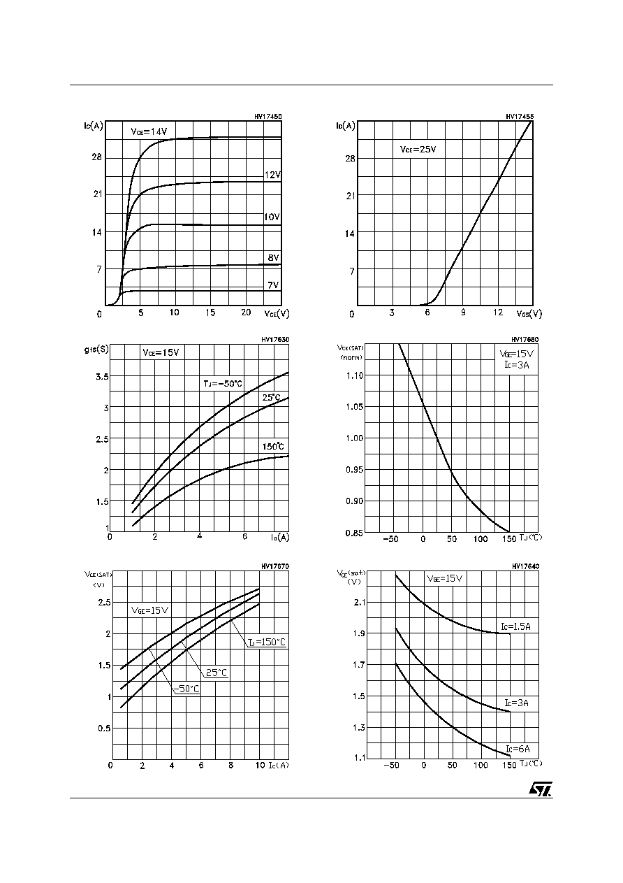
Collector-Emitter On Voltage vs Temperature
Collector-Emitter On Voltage vs Collector Current
Normalized Collector-Emitter On Voltage vs Temp.
Transconductance
Transfer Characteristics
Output Characteristics

5/11
STGP3NB60MD - STGB3NB60MD
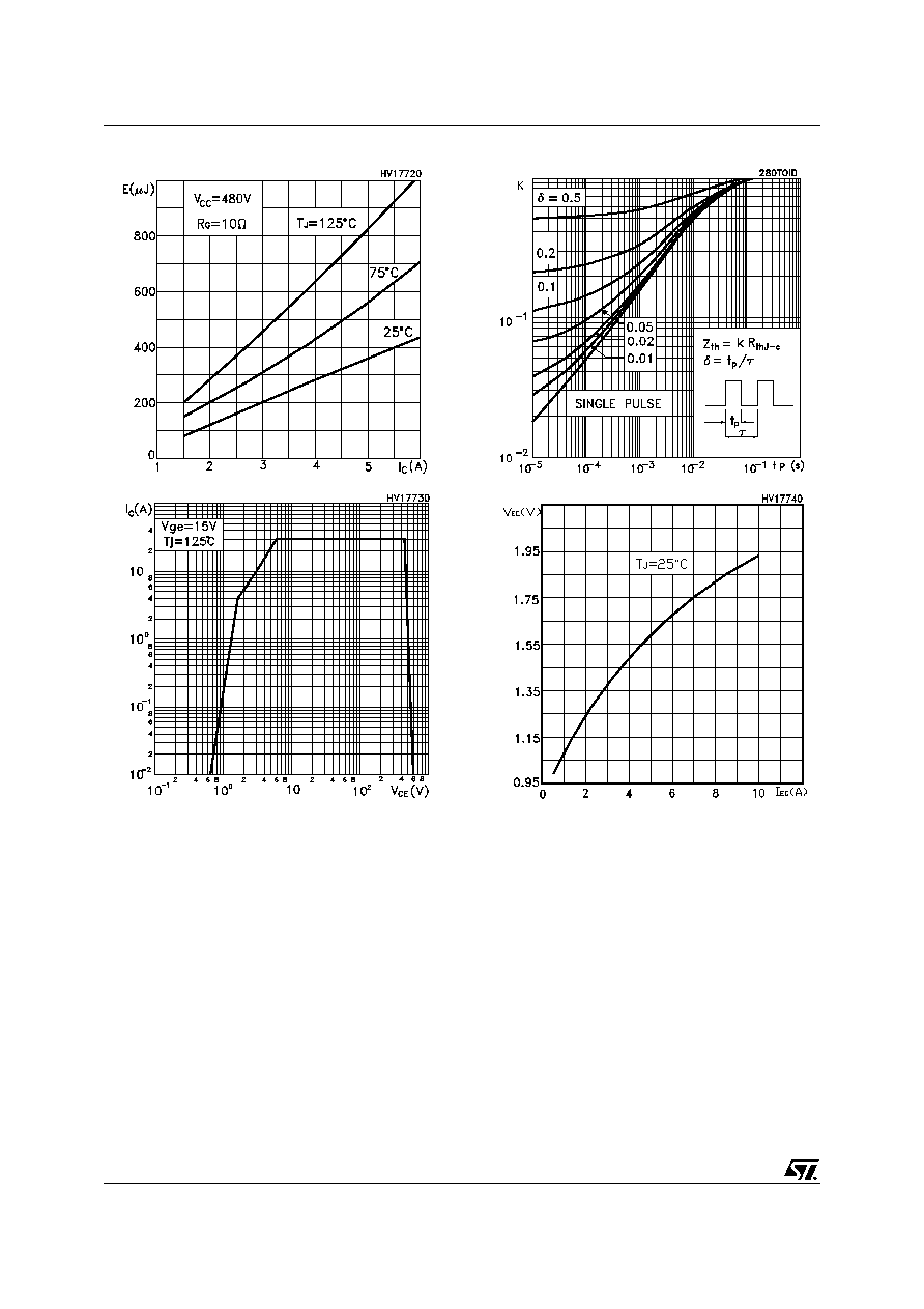
Total Switching Losses vs Temperature
Total Switching Losses vs Gate Resistance
Gate Charge vs Gate-Emitter Voltage
Capacitance Variations
Normalized Breakdown Voltage vs Temperature
Gate Threshold vs Temperature
STGP3NB60MD - STGB3NB60MD
6/11
Turn-Off SOA
Thermal Impedance for TO-220/D≤PAK
Total Switching Losses vs Collector Current
Emitter-Collector Diode Characteristics
7/11
STGP3NB60MD - STGB3NB60MD
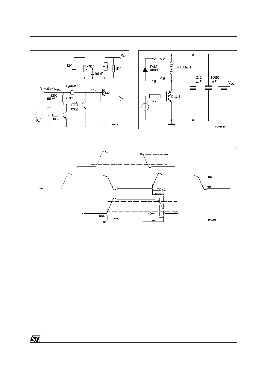
Fig. 2: Test Circuit For Inductive Load Switching
Fig. 1: Gate Charge test Circuit
STGP3NB60MD - STGB3NB60MD
8/11
DIM.
mm.
inch
MIN.
TYP
MAX.
MIN.
TYP.
MAX.
A
4.40
4.60
0.173
0.181
b
0.61
0.88
0.024
0.034
b1
1.15
1.70
0.045
0.066
c
0.49
0.70
0.019
0.027
D
15.25
15.75
0.60
0.620
E
10
10.40
0.393
0.409
e
2.40
2.70
0.094
0.106
e1
4.95
5.15
0.194
0.202
F
1.23
1.32
0.048
0.052
H1
6.20
6.60
0.244
0.256
J1
2.40
2.72
0.094
0.107
L
13
14
0.511
0.551
L1
3.50
3.93
0.137
0.154
L20
16.40
0.645
L30
28.90
1.137
¯P
3.75
3.85
0.147
0.151
Q
2.65
2.95
0.104
0.116
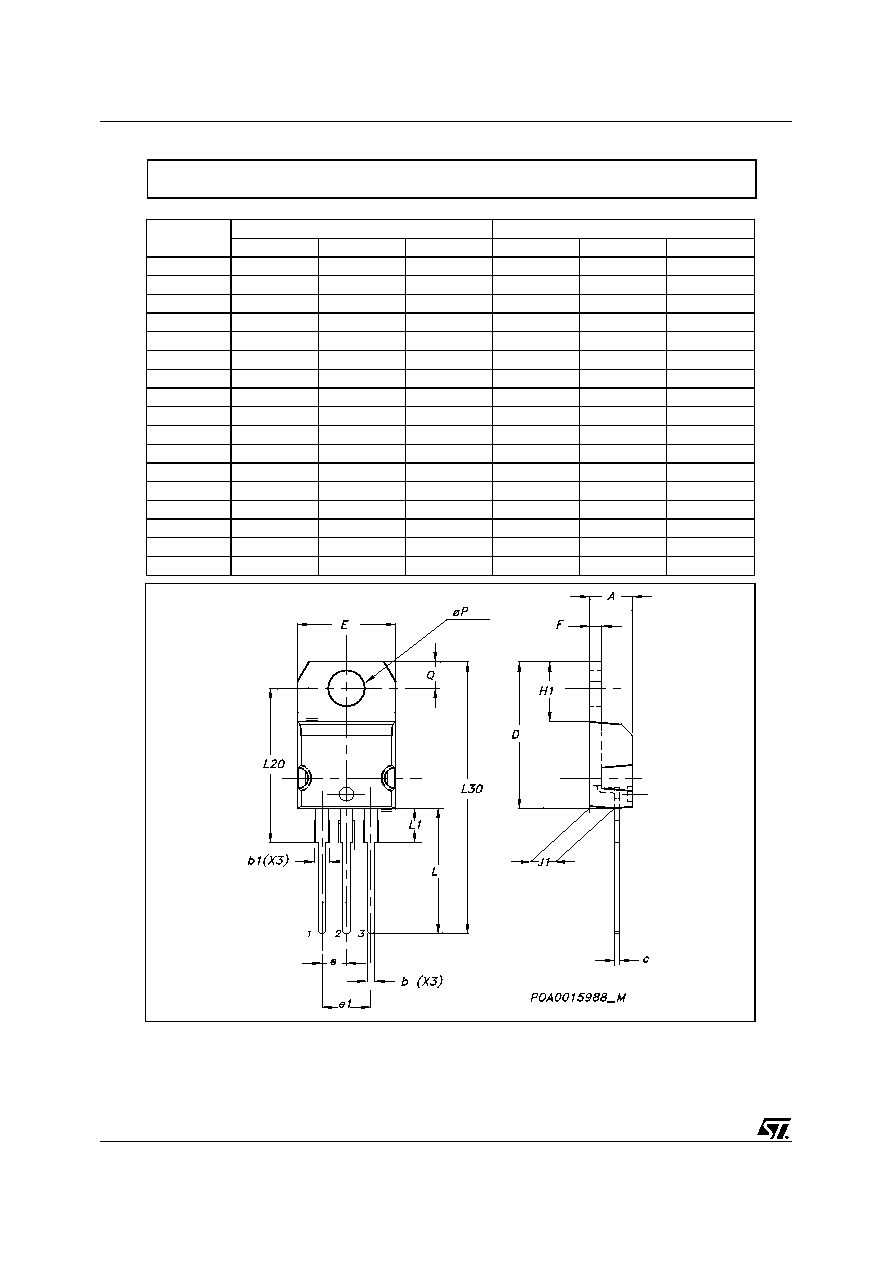
TO-220 MECHANICAL DATA
9/11
STGP3NB60MD - STGB3NB60MD
1
DIM.
mm.
inch
MIN.
TYP
MAX.
MIN.
TYP.
MAX.
A
4.4
4.6
0.173
0.181
A1
2.49
2.69
0.098
0.106
A2
0.03
0.23
0.001
0.009
B
0.7
0.93
0.027
0.036
B2
1.14
1.7
0.044
0.067
C
0.45
0.6
0.017
0.023
C2
1.23
1.36
0.048
0.053
D
8.95
9.35
0.352
0.368
D1
8
0.315
E
10
10.4
0.393
E1
8.5
0.334
G
4.88
5.28
0.192
0.208
L
15
15.85
0.590
0.625
L2
1.27
1.4
0.050
0.055
L3
1.4
1.75
0.055
0.068
M
2.4
3.2
0.094
0.126
R
0.4
0.015
V2
0∫
4∫
D
2
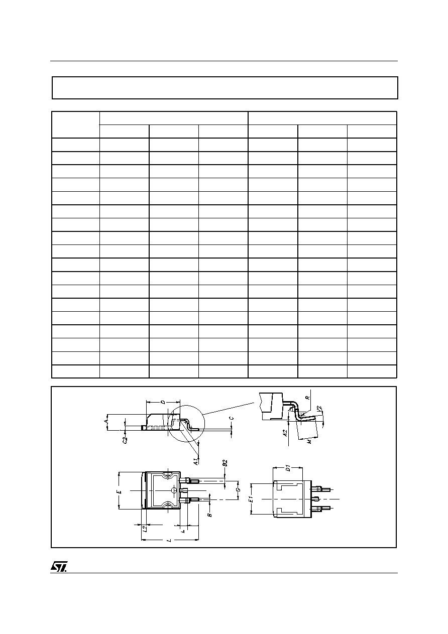
PAK MECHANICAL DATA
3
STGP3NB60MD - STGB3NB60MD
10/11
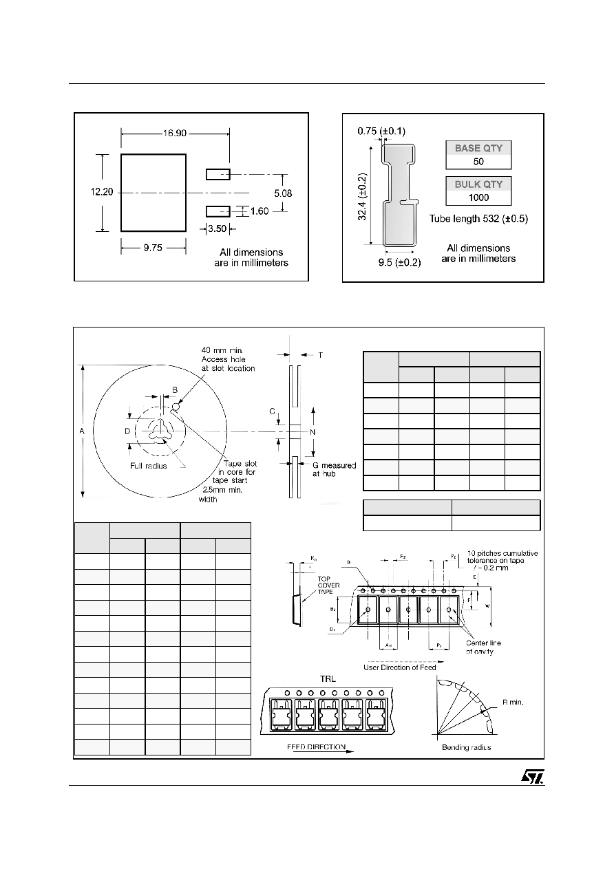
TAPE AND REEL SHIPMENT (suffix "T4")*
TUBE SHIPMENT (no suffix)*
D
2
PAK FOOTPRINT
* on sales type
DIM.
mm
inch
MIN.
MAX.
MIN.
MAX.
A
330
12.992
B
1.5
0.059
C
12.8
13.2
0.504
0.520
D
20.2
0795
G
24.4
26.4
0.960
1.039
N
100
3.937
T
30.4
1.197
BASE QTY
BULK QTY
1000
1000
REEL MECHANICAL DATA
DIM.
mm
inch
MIN.
MAX.
MIN.
MAX.
A0
10.5
10.7
0.413
0.421
B0
15.7
15.9
0.618
0.626
D
1.5
1.6
0.059
0.063
D1
1.59
1.61
0.062
0.063
E
1.65
1.85
0.065
0.073
F
11.4
11.6
0.449
0.456
K0
4.8
5.0
0.189
0.197
P0
3.9
4.1
0.153
0.161
P1
11.9
12.1
0.468
0.476
P2
1.9
2.1
0.075
0.082
R
50
1.574
T
0.25
0.35
0.0098 0.0137
W
23.7
24.3
0.933
0.956
TAPE MECHANICAL DATA

11/11
STGP3NB60MD - STGB3NB60MD
Information furnished is believed to be accurate and reliable. However, STMicroelectronics assumes no responsibility for the
consequences of use of such information nor for any infringement of patents or other rights of third parties which may result from
its use. No license is granted by implication or otherwise under any patent or patent rights of STMicroelectronics. Specifications
mentioned in this publication are subject to change without notice. This publication supersedes and replaces all information
previously supplied. STMicroelectronics products are not authorized for use as critical components in life support devices or
systems without express written approval of STMicroelectronics.
© The ST logo is a registered trademark of STMicroelectronics
© 2003 STMicroelectronics - Printed in Italy - All Rights Reserved
STMicroelectronics GROUP OF COMPANIES
Australia - Brazil - Canada - China - Finland - France - Germany - Hong Kong - India - Israel - Italy - Japan - Malaysia - Malta - Morocco
Singapore - Spain - Sweden - Switzerland - United Kingdom - United States.
© http://www.st.com