STGD3NB60SD
N-CHANNEL 3A - 600V DPAK
Power MESH
TM
IGBT
PRELIMINARY DATA
s
HIGH INPUT IMPEDANCE
(VOLTAGE DRIVEN)
s
VERY LOW ON-VOLTAGE DROP (V
cesat
)
s
HIGH CURRENT CAPABILITY
s
OFF LOSSES INCLUDE TAIL CURRENT
s
INTEGRATED FREEWHEELING DIODE
s
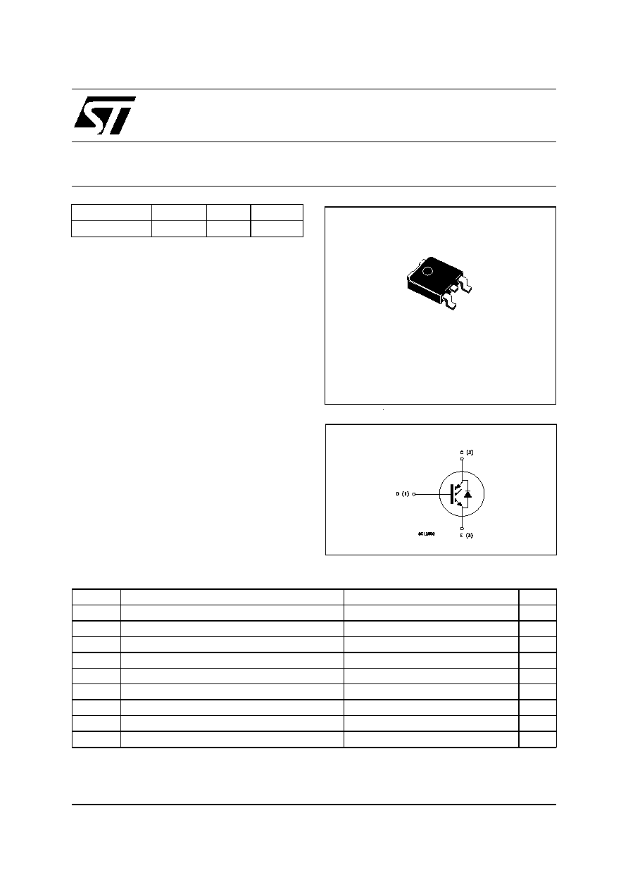
SURFACE-MOUNTING DPAK (TO-252)
POWER PACKAGE IN TAPE & REEL
(SUFFIX "T4")
DESCRIPTION
Using the latest high voltage technology based
on a patented strip layout, STMicroelectronics
has designed an advanced family of IGBTs, the
PowerMESH
TM
IGBTs, with outstanding
perfomances. The suffix "S" identifies a family
optimized to achieve minimum on-voltage drop
for low frequency applications (<1kHz).
APPLICATIONS
s
GAS DISCHARGE LAMP
s
STATIC RELAYS
s
MOTOR CONTROL
Æ
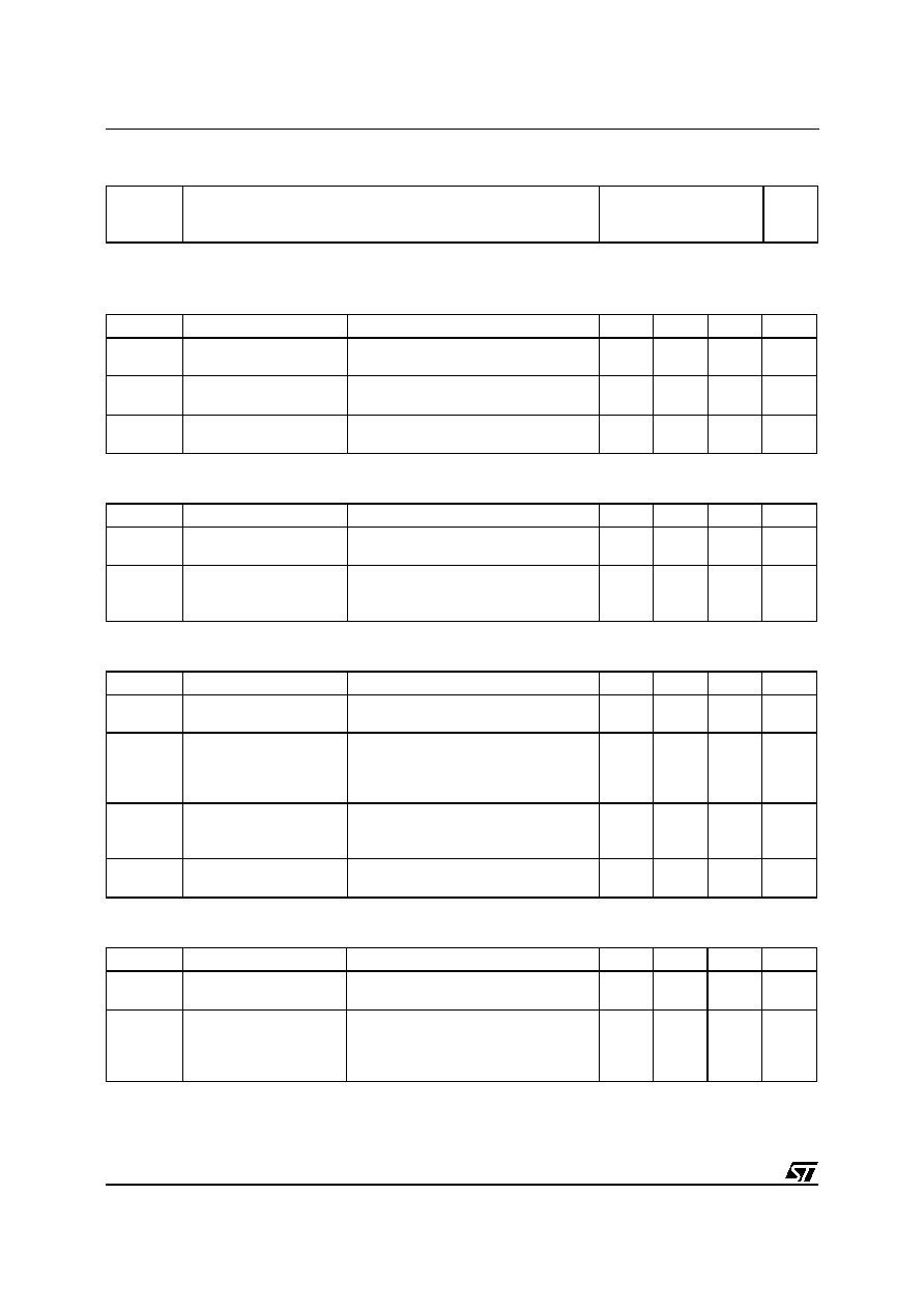
INTERNAL SCHEMATIC DIAGRAM
ABSOLUTE MAXIMUM RATINGS
Symbol
Parameter
Value
Unit
V
CES
Collector-Emitter Voltage (V
GS
= 0)
600
V
V
GE
Gate-Emitter Voltage
±
20
V
I
C
Collector Current (continuous) at T
c
= 25
o
C
6
A
I
C
Collector Current (continuous) at T
c
= 100
o
C
3
A
I
CM
(
∑
)
Collector Current (pulsed)
25
A
P
tot
Total Dissipation at T
c
= 25
o
C
48
W
Derating Factor
0.32
W/
o
C
T
stg
Storage Temperature
-65 to 175
o
C
T
j
Max. Operating Junction Temperature
175
o
C
(
∑
) Pulse width limited by safe operating area
TYPE
V
CES
V
CE(sat)
I
C
STGD3NB60SD
600 V
< 1.5 V
3 A
March 2000
1
3
DPAK
TO-252
(Suffix "T4")
1/8
THERMAL DATA
R
thj-case
R
thj-amb
R
thc-sink
Thermal Resistance Junction-case Max
Thermal Resistance Junction-ambient Max
Thermal Resistance Case-sink Typ
3.125
100
1.5
o
C/W
o
C/W
o
C/W
ELECTRICAL CHARACTERISTICS (T
j
= 25
o
C unless otherwise specified)
OFF
Symbol
Parameter
Test Conditions
Min.
Typ.
Max.
Unit
V
BR(CES)
Collector-Emitter
Breakdown Voltage
I
C
= 250
µ
A V
GE
= 0
600
V
I
CES
Collector cut-off
(V
GE
= 0)
V
CE
= Max Rating T
j
= 25
o
C
V
CE
= Max Rating T
j
= 125
o
C
10
100
µ
A
µ
A
I
GES
Gate-Emitter Leakage
Current (V
CE
= 0)
V
GE
=
±
20 V V
CE
= 0
±
100
nA
ON (
)
Symbol
Parameter
Test Conditions
Min.
Typ.
Max.
Unit
V
GE(th)
Gate Threshold
Voltage
V
CE
= V
GE
I
C
= 250
µ
A
2.5
5
V
V
CE(SAT)
Collector-Emitter
Saturation Voltage
V
GE
= 15 V I
C
= 1.5 A
V
GE
= 15 V I
C
= 3 A
V
GE
= 15 V I
C
= 3 A T
j
= 125
o
C
1
1.2
1.1
1.5
V
V
V
DYNAMIC
Symbol
Parameter
Test Conditions
Min.
Typ.
Max.
Unit
g
f s
Forward
Transconductance
V
CE
=25 V I
C
= 3 A
1.7
2.5
S
C
ies
C
oes
C
res
Input Capacitance
Output Capacitance
Reverse Transfer
Capacitance
V
CE
= 25 V f = 1 MHz V
GE
= 0
255
30
5.6
330
40
7
pF
pF
pF
Q
G
Q
GE
Q
GC
Total Gate Charge
Gate-Emitter Charge
Gate-Collector Charge
V
CE
= 480 V I
C
= 3 A V
GE
= 15 V
18
5.4
5.5
nC
nC
nC
I
CL
Latching Current
V
clamp
= 480 V R
G
=1k
T
j
= 150
o
C
12
A
SWITCHING ON
Symbol
Parameter
Test Conditions
Min.
Typ.
Max.
Unit
t
d(on )
t
r
Delay Time
Rise Time
V
CC
= 480 V I
C
= 3 A
V
GE
= 15 V R
G
= 1k
125
150
ns
ns
(di/dt)
on
E
on
Turn-on Current Slope
Turn-on Switching
Losses
V
CC
= 480 V I
C
= 3 A
R
G
= 1k
V
GE
= 15 V
T
j
= 125
o
C
50
1100
A/
µ
s
µ
J
STGD3NB60SD
2/8
ELECTRICAL CHARACTERISTICS (continued)
SWITCHING OFF
Symbol
Parameter
Test Conditions
Min.
Typ.
Max.
Unit
t
c
t
r
(v
off
)
t
d
(
of f
)
t
f
E
off
(**)
Cross-Over Time
Off Voltage Rise Time
Delay Time
Fall Time
Turn-off Switching Loss
V
CC
= 480 V I
C
= 3 A
R
GE
= 1 k
V
GE
= 15 V
1.8
1.0
3.4
0.72
1.15
µ
s
µ
s
µ
s
µ
s
mJ
t
c
t
r
(v
off
)
t
d
(
of f
)
t
f
E
off
(**)
Cross-Over Time
Off Voltage Rise Time
Delay Time
Fall Time
Turn-off Switching Loss
V
CC
= 480 V I
C
= 3 A
R
GE
= 1k
V
GE
= 15 V
T
j
= 125
o
C
2.8
1.45
3.6
1.2
1.8
µ
s
µ
s
µ
s
µ
s
mJ
COLLECTOR-EMITTER DIODE
Symbol
Parameter
Test Conditions
Min.
Typ.
Max.
Unit
I
f
I
fm
Forward Current
Forward Current pulsed
3
25
A
A
V
f
Forward On-Voltage
I
f
= 3 A
I
f
= 1 A
1.55
1.15
1.9
V
V
t
rr
Q
rr
I
rrm
Reverse Recovery Time
Reverse Recovery Charge
Reverse Recovery Current
I
f
= 3 A V
R
=200 V
dI/dt = 100 A/
µ
S T
j
= 125
o
C
1700
4500
9.5
ns
nC
A
(
∑
) Pulse width limited by max. junction temperature
(
) Pulsed: Pulse duration = 300
µ
s, duty cycle 1.5 %
(**)Losses Include Also The Tail (Jedec Standardization)
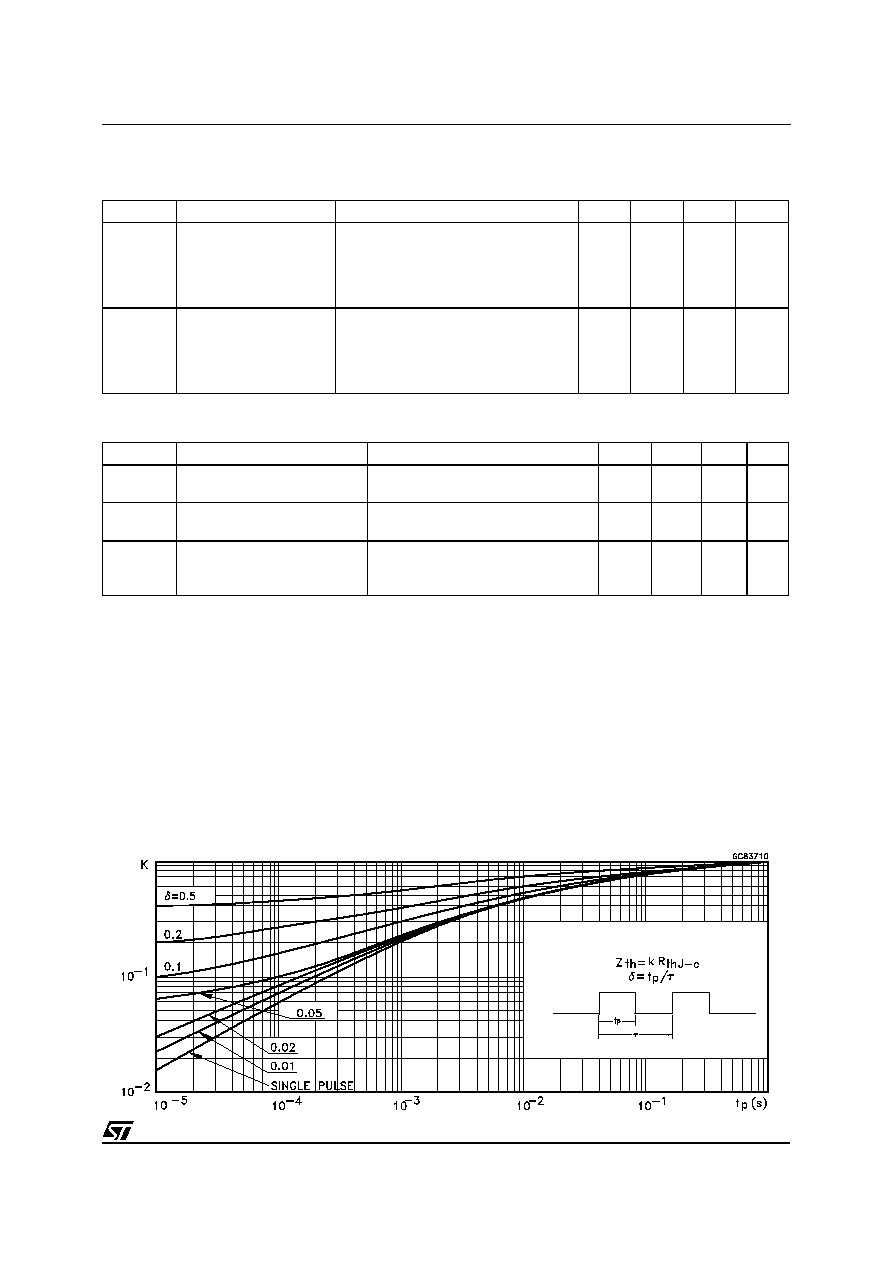
Thermal Impedance
STGD3NB60SD
3/8
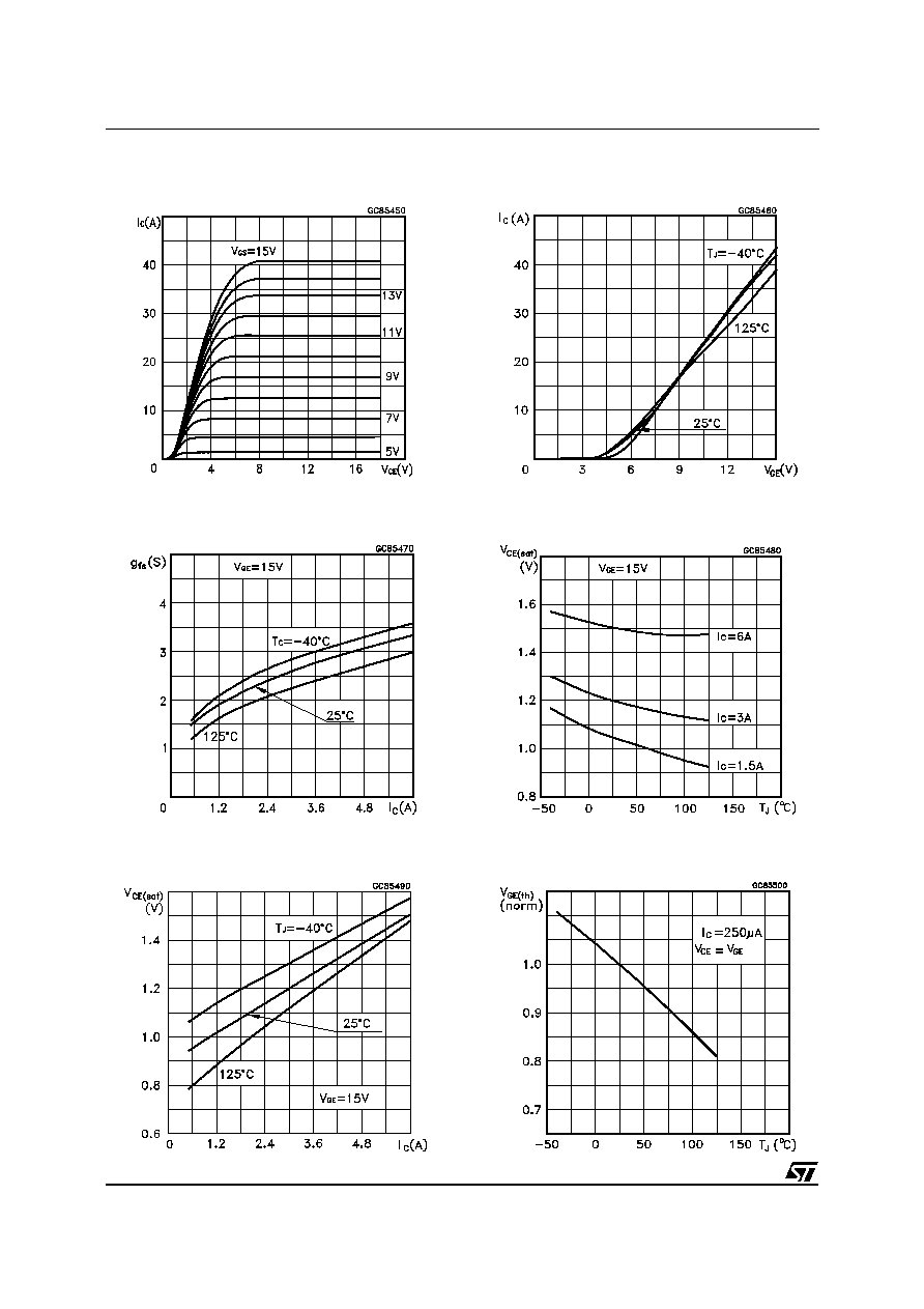
Output Characteristics
Transconductance
Collector-Emitter On Voltage vs Collector Current
Transfer Characteristics
Collector-Emitter On Voltage vs Temperature
Gate Threshold vs Temperature
STGD3NB60SD
4/8
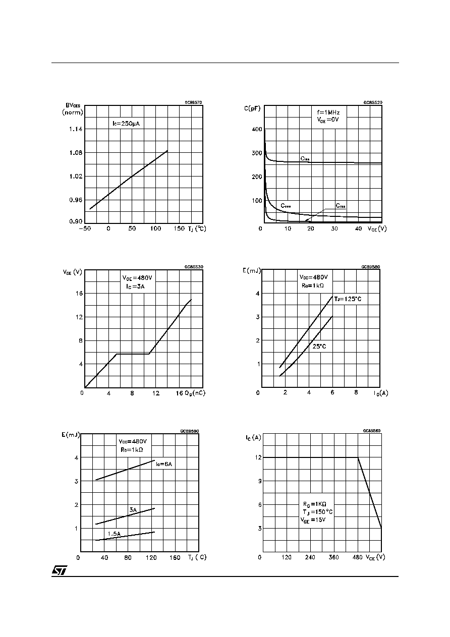
Normalized Breakdown Voltage vs Temperature
Gate Charge vs Gate-Emitter Voltage
Off Switching Losses vs Tj
Capacitance Variations
Off Switching Losses vs Ic
Switching Off Safe Operatin Area
STGD3NB60SD
5/8
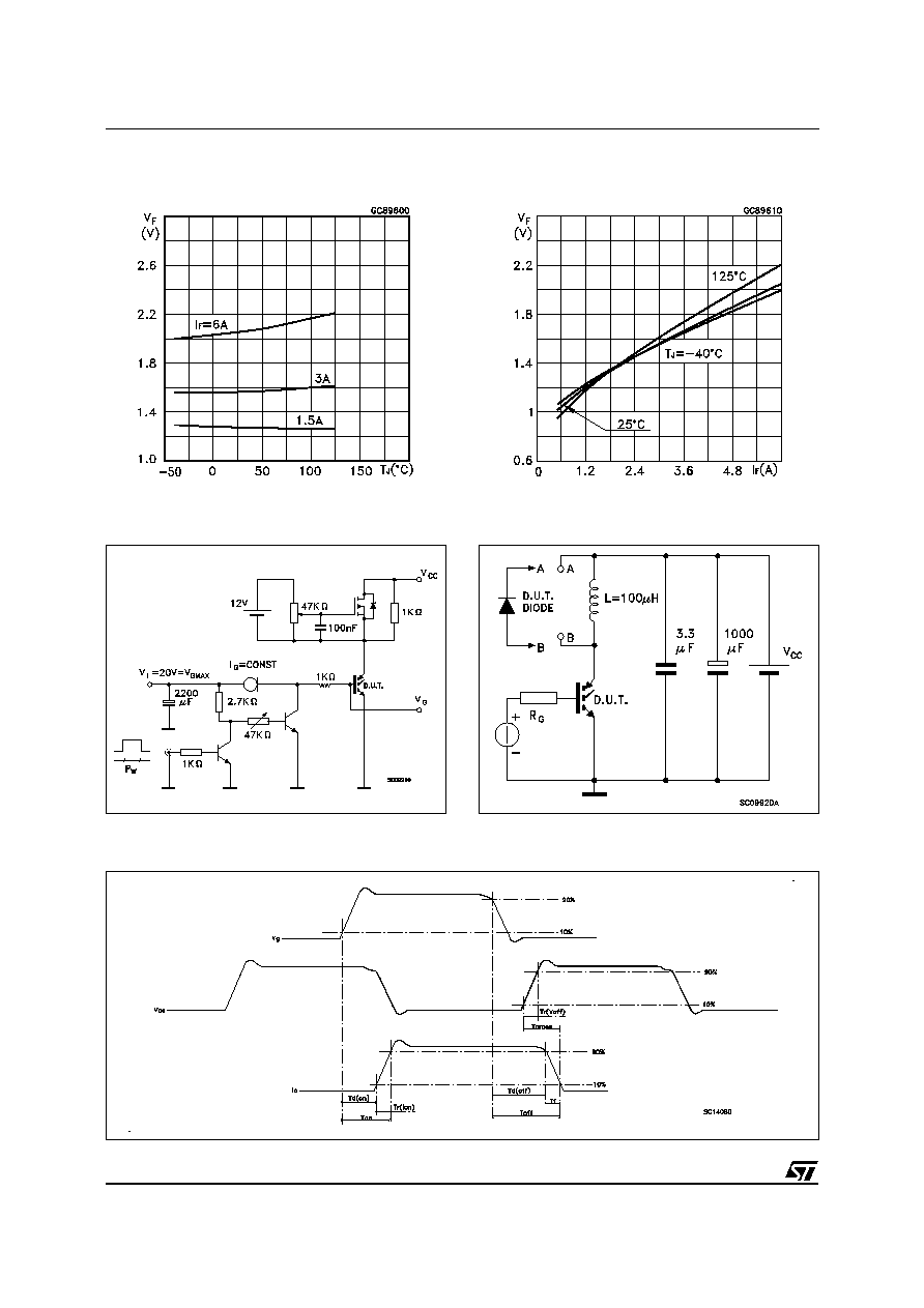
Diode Forward vs Tj
Diode Forward Voltage
Fig. 1: Gate Charge test Circuit
Fig. 3: Switching Waveforms
Fig. 2: Test Circuit For Inductive Load Switching
STGD3NB60SD
6/8
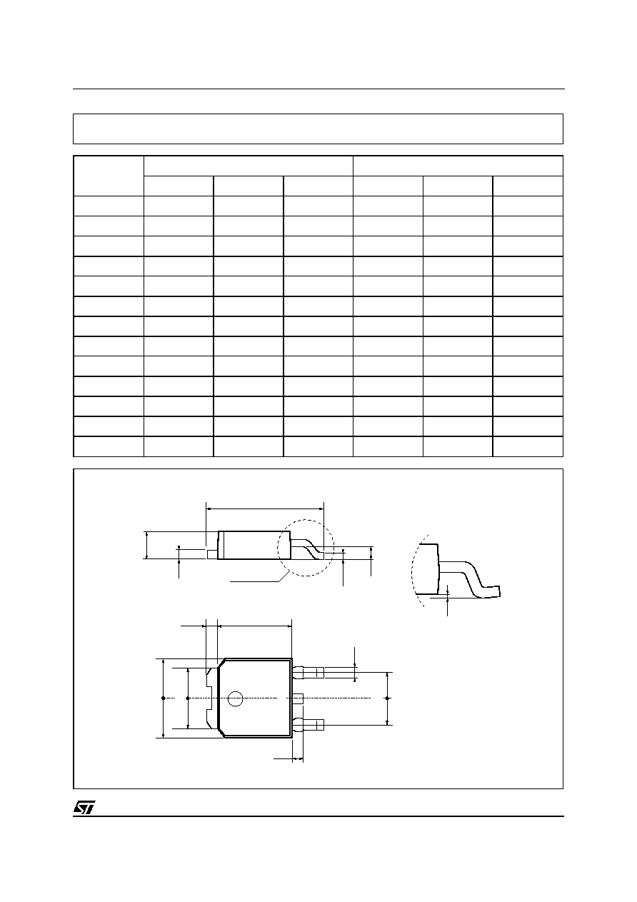
DIM.
mm
inch
MIN.
TYP.
MAX.
MIN.
TYP.
MAX.
A
2.2
2.4
0.086
0.094
A1
0.9
1.1
0.035
0.043
A2
0.03
0.23 0.001
0.009
B
0.64
0.9
0.025
0.035
B2
5.2
5.4
0.204
0.212
C
0.45
0.6
0.017
0.023
C2
0.48
0.6
0.019
0.023
D
6
6.2
0.236
0.244
E
6.4
6.6
0.252
0.260
G
4.4
4.6
0.173
0.181
H
9.35
10.1
0.368
0.397
L2
0.8
0.031
L4
0.6
1
0.023
0.039
==
D
L2
L4
1 3
==
B
E
==
B2
G
2
A
C2
C
H
A1
DETAIL "A"
A2
DETAIL "A"
TO-252 (DPAK) MECHANICAL DATA
0068772-B
STGD3NB60SD
7/8

Information furnished is believed to be accurate and reliable. However, STMicroelectronics assumes no responsibility for the consequences
of use of such information nor for any infringement of patents or other rights of third parties which may result from its use. No license is
granted by implication or otherwise under any patent or patent rights of STMicroelectronics. Specification mentioned in this publication are
subject to change without notice. This publication supersedes and replaces all information previously supplied. STMicroelectronics products
are not authorized for use as critical components in life support devices or systems without express written approval of STMicroelectronics.
The ST logo is a trademark of STMicroelectronics
© 1999 STMicroelectronics ≠ Printed in Italy ≠ All Rights Reserved
STMicroelectronics GROUP OF COMPANIES
Australia - Brazil - China - Finland - France - Germany - Hong Kong - India - Italy - Japan - Malaysia - Malta - Morocco -
Singapore - Spain - Sweden - Switzerland - United Kingdom - U.S.A.
http://www.st.com
.
STGD3NB60SD
8/8