1/9
June 2003
STGE200NB60S
N-CHANNEL 150A - 600V
- ISOTOP
PowerMESHTM IGBT
s
HIGH INPUT IMPEDANCE (VOLTAGE DRIVEN)
s
LOW ON-VOLTAGE DROP (V
cesat
)
s
OFF LOSSES INCLUDE TAIL CURRENT
s
LOW GATE CHARGE
s
HIGH CURRENT CAPABILITY
DESCRIPTION
Using the latest high voltage technology based on a
patented strip layout, STMicroelectronics has
designed an advanced family of IGBTs, the
PowerMESH
TM
IGBTs, with outstanding
performances. The suffix "S" identifies a family
optimized to achieve very low
V
CE(sat)
(@ max
frequency of 1KHz).
APPLICATIONS
s
LOW FREQUENCY MOTOR CONTROLS
s
ALUMINUM WELDING EQUIPMENT
ABSOLUTE MAXIMUM RATINGS
( ) PULSE WIDTH LIMITED BY SAFE OPERATING AREA
TYPE
V
CES
V
CE(sat)
(typ.)
I
C
T
C
STGE200NB60S
600 V
1.2
V
1.3
V
150 A
200 A
100∞C
25∞C
Symbol
Parameter
Value
Unit
V
CES
Collector-Emitter Voltage (V
GS
= 0)
600
V
V
GE
Gate-Emitter Voltage
±20
V
I
C
Collector Current (continuous) at T
C
= 25∞C
200
A
I
C
Collector Current (continuous) at T
C
= 100∞C
150
A
I
CM
( )
Collector Current (pulsed)
400
A
P
TOT
Total Dissipation at T
C
= 25∞C
600
W
Derating Factor
4.8
W/∞C
T
stg
Storage Temperature
≠ 65 to 150
∞C
T
j
Max. Operating Junction Temperature
150
∞C
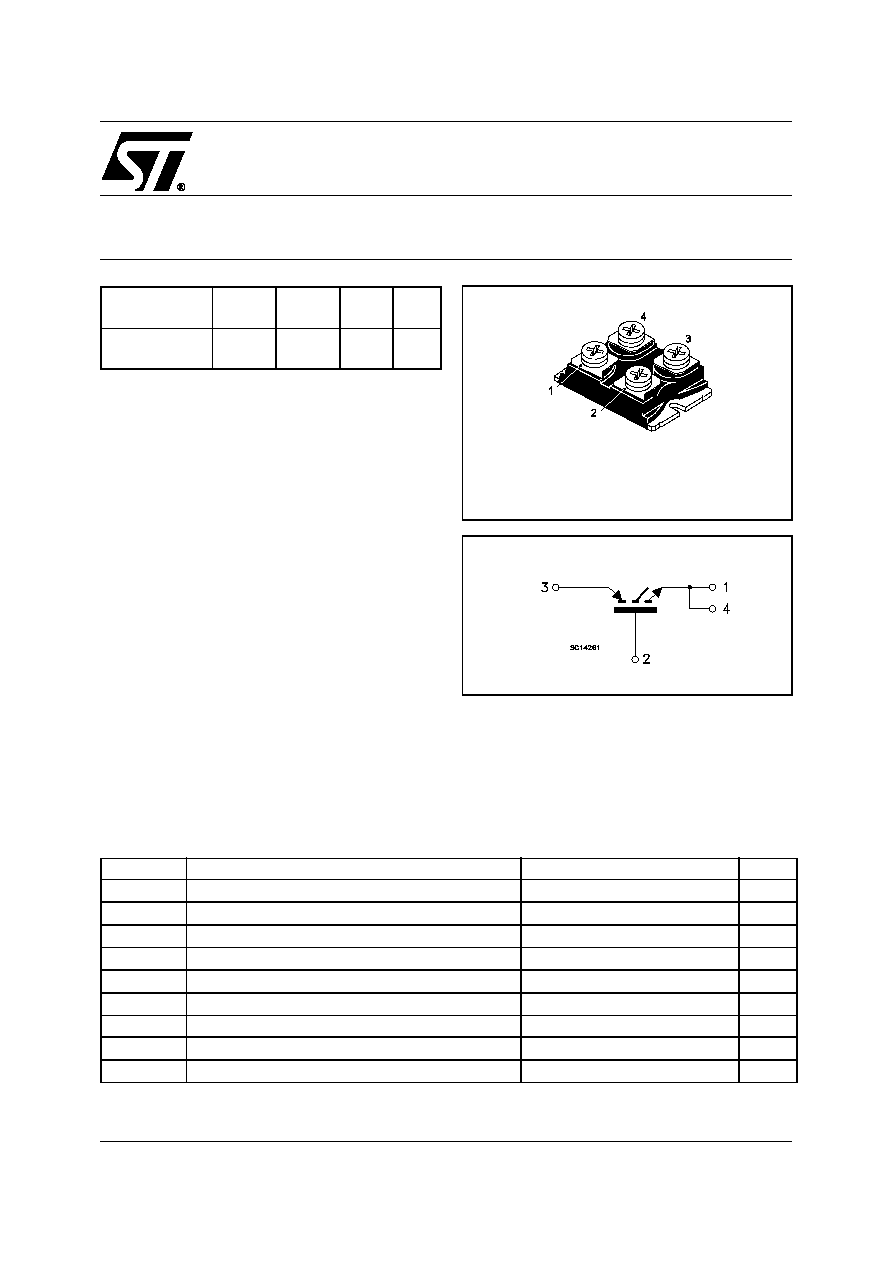
ISOTOP
INTERNAL SCHEMATIC DIAGRAM
STGE200NB60S
2/9
THERMAL DATA
ELECTRICAL CHARACTERISTICS (T
CASE
= 25 ∞C UNLESS OTHERWISE SPECIFIED)
OFF
ON (1)
DYNAMIC
SWITCHING ON
ELECTRICAL CHARACTERISTICS (CONTINUED)
Rthj-case
Thermal Resistance Junction-case Max
0.208
∞C/W
Rthj-amb
Thermal Resistance Junction-ambient Max
30
∞C/W
Symbol
Parameter
Test Conditions
Min.
Typ.
Max.
Unit
V
BR(CES)
Collector-Emitter Breakdown
Voltage
I
C
= 250 µA, V
GE
= 0
600
V
I
CES
Collector cut-off
(V
GE
= 0)
V
CE
= Max Rating, T
C
= 25 ∞C
500
µA
V
CE
= Max Rating, T
C
= 125 ∞C
5
mA
I
GES
Gate-Emitter Leakage
Current (V
CE
= 0)
V
GE
= ±20V , V
CE
= 0
±100
nA
Symbol
Parameter
Test Conditions
Min.
Typ.
Max.
Unit
V
GE(th)
Gate Threshold Voltage
V
CE
= V
GE
, I
C
= 250µA
3
5
V
V
CE(sat)
Collector-Emitter Saturation
Voltage
V
GE
= 15V, I
C
= 100 A
1.2
1.6
V
V
GE
= 15V, I
C
=150 A, Tj =100∞C
1.2
V
Symbol
Parameter
Test Conditions
Min.
Typ.
Max.
Unit
g
fs
Forward Transconductance
V
CE
= 15 V
,
I
C
= 100 A
80
S
C
ies
C
oes
C
res
Input Capacitance
Output Capacitance
Reverse Transfer
Capacitance
V
CE
= 25V, f = 1 MHz, V
GE
= 0
15600
1100
95
pF
pF
pF
Q
g
Q
ge
Q
gc
Total Gate Charge
Gate-Emitter Charge
Gate-Collector Charge
V
CE
= 480V, I
C
= 100 A,
V
GE
= 15V
560
70
170
nC
nC
nC
I
CL
Latching Current
V
clamp
= 480 V
Tj = 125∞C , R
G
= 10
300
A
Symbol
Parameter
Test Conditions
Min.
Typ.
Max.
Unit
t
d(on)
t
r
Turn-on Delay Time
Rise Time
V
CC
= 480 V, I
C
= 100 A
R
G
= 2
, V
GE
= 15 V
64
112
µs
µs
(di/dt)
on
Eon
Turn-on Current Slope
Turn-on Switching Losses
V
CC
= 480 V, I
C
= 100 A R
G
=2
V
GE
= 15 V,Tj = 125∞C
1800
12
A/µs
mJ
3/9
STGE200NB60S
SWITCHING OFF
Note: 1. Pulsed: Pulse duration = 300 µs, duty cycle 1.5 %.
2. Pulse width limited by max. junction temperature.
(**)Losses include Also the Tail (Jedec Standardization)
Symbol
Parameter
Test Conditions
Min.
Typ.
Max.
Unit
t
c
Cross-over Time
V
cc
= 480 V, I
C
= 100 A,
R
GE
= 2
, V
GE
= 15 V
2.98
µs
t
r
(V
off
)
Off Voltage Rise Time
1.7
µs
t
d
(
off
)
Delay Time
2.4
µs
t
f
Fall Time
1.23
µs
E
off
(**)
Turn-off Switching Loss
59
mJ
E
ts
Total Switching Loss
71
mJ
t
c
Cross-over Time
V
cc
= 480 V, I
C
= 100 A,
R
GE
= 2
, V
GE
= 15 V
Tj = 125 ∞C
4.52
µs
t
r
(V
off
)
Off Voltage Rise Time
2.6
µs
t
d
(
off
)
Delay Time
2.8
µs
t
f
Fall Time
1.8
µs
E
off
(**)
Turn-off Switching Loss
92
mJ
E
ts
Total Switching Loss
105
mJ
STGE200NB60S
4/9
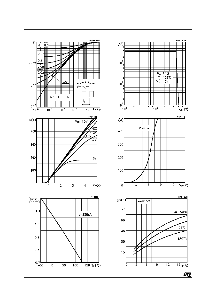
Normalized Gate Threshold Voltage vs Temp.
Transconductance
Transfer Characteristics
Switching Off Safe Operating Area
Output Characteristics
Thermal Impedance

5/9
STGE200NB60S
Total Switching losses vs Temperature
Total Switching losses vs Gate Resistance
Capacitance Variations
Normalized Break-down Voltage vs Temp.
Gate-Charge vs Gate-Emitter Voltage
Collector-Emitter On Voltage vs Temperature